Chapter 5. PowerPC Processor Core
5-15
Programming Model
16
ICE
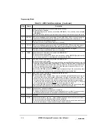
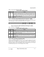
Instruction cache enable
2
0 The instruction cache is neither accessed nor updated. All pages are accessed as if they
were marked cache-inhibited (WIM = X1X). Potential cache accesses from the bus (snoop
and cache operations) are ignored. In the disabled state for the L1 caches, the cache tag
state bits are ignored, and all accesses are propagated to the bus as single-beat transactions.
For these transactions, however, the processor reflects the original state of the I bit (from the
MMU) to the peripheral logic block, regardless of cache disabled status.
ICE is zero at power-up.
1 The instruction cache is enabled.
17
DCE
Data cache enable
2
0 The data cache is neither accessed nor updated. All pages are accessed as if they were
marked cache-inhibited (WIM = X1X). Potential cache accesses from the bus (snoop and
cache operations) are ignored. In the disabled state, the cache tag state bits are ignored and
all accesses are propagated to the bus as single-beat transactions.
For those transactions, however, the processor reflects the original state of the I bit (from the
MMU) to the peripheral logic block, regardless of cache disabled status.
DCE is zero at power-up.
1 The data cache is enabled.
18
ILOCK
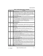
Instruction cache lock
0 Normal operation
1 Instruction cache is locked. A locked cache supplies data normally on a hit, but an access is
treated as a cache-inhibited transaction on a miss. On a miss, the transaction to the bus is
single-beat.
To prevent locking during a cache access, an isync must precede the setting of ILOCK.
19
DLOCK
Data cache lock
0 Normal operation
1 Data cache is locked. A locked cache supplies data normally on a hit but an access is treated
as a cache-inhibited transaction on a miss. On a miss, the transaction to the bus is
single-beat.
A snoop hit to a locked L1 data cache performs as if the cache were not locked. A cache block
invalidated by a snoop remains invalid until the cache is unlocked.
To prevent locking during a cache access, a sync must precede the setting of DLOCK.
20
ICFI
Instruction cache flash invalidate
2
0 The instruction cache is not invalidated. The bit is cleared when the invalidation operation
begins (usually the next cycle after the write operation to the register). The instruction cache
must be enabled for the invalidation to occur.
1 An invalidate operation is issued that marks the state of each instruction cache block as
invalid without writing back modified cache blocks to memory. Cache access is blocked during
this time. Accesses to the cache from the peripheral logic bus are signaled as a miss during
invalidate-all operations. Setting ICFI clears all the valid bits of the blocks and the PLRU bits
to point to way L0 of each set.
For 603e processors, the proper use of the ICFI and DCFI bits is to set them and clear them
with two consecutive mtspr operations.
21
DCFI
Data cache flash invalidate
2
0 The data cache is not invalidated. The bit is cleared when the invalidation operation begins
(usually the next cycle after the write operation to the register). The data cache must be
enabled for the invalidation to occur.
1 An invalidate operation is issued that marks the state of each data cache block as invalid
without writing back modified cache blocks to memory. Cache access is blocked during this
time. Accesses to the cache from the peripheral logic bus are signaled as a miss during
invalidate-all operations. Setting DCFI clears all the valid bits of the blocks and the PLRU bits
so that they point to way L0 of each set.
For 603e processors, the proper use of the ICFI and DCFI bits is to set them and clear them
with two consecutive mtspr operations.
22–23
—
Reserved
Table 5-1. HID0 Field Descriptions (Continued)
Bits
Name
Description
Summary of Contents for MPC8240
Page 1: ...MPC8240UM D Rev 1 1 2001 MPC8240 Integrated Processor User s Manual ...
Page 38: ...xviii MPC8240 Integrated Processor User s Manual TABLES Table Number Title Page Number ...
Page 48: ...xlviii MPC8240 Integrated Processor User s Manual Acronyms and Abbreviations ...
Page 312: ...6 94 MPC8240 Integrated Processor User s Manual ROM Flash Interface Operation ...
Page 348: ...7 36 MPC8240 Integrated Processor User s Manual PCI Host and Agent Modes ...
Page 372: ...8 24 MPC8240 Integrated Processor User s Manual DMA Register Descriptions ...
Page 394: ...9 22 MPC8240 Integrated Processor User s Manual I2O Interface ...
Page 412: ...10 18 MPC8240 Integrated Processor User s Manual Programming Guidelines ...
Page 454: ...12 14 MPC8240 Integrated Processor User s Manual Internal Arbitration ...
Page 466: ...13 12 MPC8240 Integrated Processor User s Manual Exception Latencies ...
Page 516: ...16 14 Watchpoint Trigger Applications ...
Page 538: ...B 16 MPC8240 Integrated Processor User s Manual Setting the Endian Mode of Operation ...
Page 546: ...C 8 MPC8240 Integrated Processor User s Manual ...
Page 640: ...INDEX Index 16 MPC8240 Integrated Processor User s Manual ...

