Chapter 6. MPC8240 Memory Interface
6-81
ROM/Flash Interface Operation
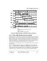
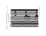
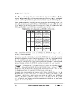
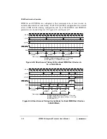
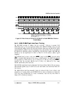
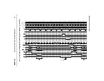
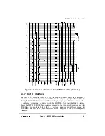
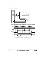
Figure 6-57. Read Access Timing (Cache Block) for Burst ROM/Flash Devices
in 32-Bit Mode
6.4.3 8-Bit ROM/Flash Interface Timing
The MPC8240 provides 21 address bits for accessing 2 Mbytes of external 8-bit
ROM/Flash memory. The most significant address bit is SDMA12/SDBA1. The next eight
most significant address bits are provided as an alternate function on the MPC8240’s parity
signals, PAR[0:7] (AR[19:12]). The remaining 12 low-order address bits are provided on
the MPC8240’s SDBA[0] (AR[11]) and SDMA[10:0] (AR[10:0]) signals with SDMA[0]
(AR[0]) as the least significant bit. Refer to Table 6-2 for the memory address signal
mappings.
The MPC8240 also provides a chip select (RCS0), output enable (FOE), and write enable
(WE) to facilitate both read and write accesses to Flash memory. The MPC8240 supports
x8 organizations of Flash memory up to a total space of 2 Mbytes. Chip select RCS0 is
decoded from the memory address, and is active for addresses in the range
0xFF80_0000–FFFF_FFFF for Flash.
The MPC8240 performs byte-lane alignment for byte reads from Flash (x8) boot memory.
The MPC8240 gathers bytes for half-word, word, and double-word reads from Flash (x8)
boot memory.
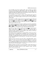
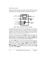
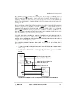
The MPC8240 provides programmable timing for read and write access to Flash, with
granularity of 1 system clock cycle. ROMFAL[0–4] is used to determine read and write
cycle wait states. ROMNAL[0–3] is used to determine write recovery time. Refer to
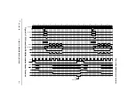
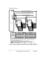
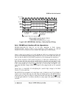
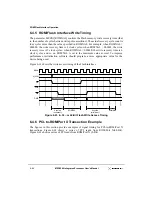
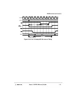
Figure 6-58 for further information.
MCLK
A[0:1]
A[2:19]
FOE,
DATA
ROMNAL
Data sampled
ROMFAL (ROM first access latency) = 3–34 clocks
MCCR1[BURST] = 1
D0
ROMNAL
ROMNAL
ROMNAL (ROM nibble access latency) = 0–9 clocks
D1
D2
D3
D4
D5
D6
D7
ROMFAL
ROMNAL
ROMNAL
ROMNAL
ROMNAL
RCSn
Summary of Contents for MPC8240
Page 1: ...MPC8240UM D Rev 1 1 2001 MPC8240 Integrated Processor User s Manual ...
Page 38: ...xviii MPC8240 Integrated Processor User s Manual TABLES Table Number Title Page Number ...
Page 48: ...xlviii MPC8240 Integrated Processor User s Manual Acronyms and Abbreviations ...
Page 312: ...6 94 MPC8240 Integrated Processor User s Manual ROM Flash Interface Operation ...
Page 348: ...7 36 MPC8240 Integrated Processor User s Manual PCI Host and Agent Modes ...
Page 372: ...8 24 MPC8240 Integrated Processor User s Manual DMA Register Descriptions ...
Page 394: ...9 22 MPC8240 Integrated Processor User s Manual I2O Interface ...
Page 412: ...10 18 MPC8240 Integrated Processor User s Manual Programming Guidelines ...
Page 454: ...12 14 MPC8240 Integrated Processor User s Manual Internal Arbitration ...
Page 466: ...13 12 MPC8240 Integrated Processor User s Manual Exception Latencies ...
Page 516: ...16 14 Watchpoint Trigger Applications ...
Page 538: ...B 16 MPC8240 Integrated Processor User s Manual Setting the Endian Mode of Operation ...
Page 546: ...C 8 MPC8240 Integrated Processor User s Manual ...
Page 640: ...INDEX Index 16 MPC8240 Integrated Processor User s Manual ...

