INDEX
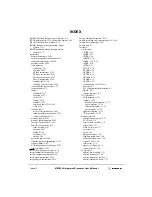
Index-2
MPC8240 Integrated Processor User’s Manual
condition register logical, D-24
system linkage, D-24
trap, D-24
Buffers
internal buffers
copy-back buffer, 12-2
PCI/local memory buffers, 12-6
PCI-to-local-memory-read (PCMRBs), 12-7
PCI-to-local-memory-write (PCMWBs), 12-8
processor-to-PCI-read buffer (PRPRB), 12-4
processor-to-PCI-write buffers (PRPWBs), 12-5
Burst operations
burst ordering
PCI cache wrap mode, 7-12
PCI linear incrementing, 7-12
Bus interface
bus ratios, 1-17
PCI bus arbitration, 1-14
peripheral logic bus, 1-10
peripheral logic bus interface, 5-9
Bus operations
PCI bus transactions, see PCI interface
alignment, 7-13, B-2
byte enable signals, 2-10, 7-12, 7-13
ordering
big-endian mode, B-2
little-endian mode, B-5
mechanisms, B-1
most-significant byte/bit (MSB/msb), B-1
PCI bus, 7-2, B-1
processor bus, B-1
Byte-reverse instructions, D-22
C
C/BEn (command/byte enable)
Cache
cache coherency, 5-24
cache managment instructions, D-25
central control unit (CCU), 5-24
chance wrap mode, PCI, 7-12
overview, 5-9
processor core cache implementation, 5-20
CASn (column address strobe) signals, 2-17
CDAR (current descriptor address) register, 8-19
CDCR (clock driver control) register, 4-20
Central control unit (CCU)
cache coherency, 5-24
overview, 12-1
Chaining mode
CHKSTOP_IN (checkstop in), 2-28
CKE (SDRAM clock enable) signal, 2-21
CKO (test clock) signal, 2-34
Clocks
clock stretching, 10-7
clock subsystem block diagram, 2-34
clock synchronization, 2-36, 10-6
clocking method, 2-34
clocking on the MPC107, 2-34
DLL operation and locking, 2-35
examples, 2-37
signal description, 2-32
signals see Signals, clock, 2-32
Commands
mode-set command, 6-26
PCI commands
C/BEn signals, 7-9
C/BEn signals, 2-10
encodings, 7-9
interrupt-acknowledge transaction, 7-27
PCI command register, 4-11
special-cycle command, 7-28
Compare instructions, D-18
Completion, PCI, 7-17
Configuration
configuration registers
CONFIG_ADDR register, 7-23
CONFIG_DATA register, 7-23
ECC single-bit error registers, 13-7
emulation support, 4-41
error detection registers, 13-5
error handling registers, 4-33
60x/PCI error address register, 4-40
bus error status register, 4-34
ECC single-bit error registers, 4-33, 4-34
error detection registers, 4-35
error enabling registers, 4-34
PCI bus error status register, 4-40
processor bus error status register, 4-37
error status registers, 4-39
memory interface
memory bank enable register, 4-27
memory boundary registers, 4-23–4-27
memory control configuration registers, 4-42
memory page mode register, 4-28
PCI registers, see Registers, PCI
power management registers, ??–4-18
processor bus error status
processor interface registers, 4-29
processor/PCI error address register, 13-6
Summary of Contents for MPC8240
Page 1: ...MPC8240UM D Rev 1 1 2001 MPC8240 Integrated Processor User s Manual ...
Page 38: ...xviii MPC8240 Integrated Processor User s Manual TABLES Table Number Title Page Number ...
Page 48: ...xlviii MPC8240 Integrated Processor User s Manual Acronyms and Abbreviations ...
Page 312: ...6 94 MPC8240 Integrated Processor User s Manual ROM Flash Interface Operation ...
Page 348: ...7 36 MPC8240 Integrated Processor User s Manual PCI Host and Agent Modes ...
Page 372: ...8 24 MPC8240 Integrated Processor User s Manual DMA Register Descriptions ...
Page 394: ...9 22 MPC8240 Integrated Processor User s Manual I2O Interface ...
Page 412: ...10 18 MPC8240 Integrated Processor User s Manual Programming Guidelines ...
Page 454: ...12 14 MPC8240 Integrated Processor User s Manual Internal Arbitration ...
Page 466: ...13 12 MPC8240 Integrated Processor User s Manual Exception Latencies ...
Page 516: ...16 14 Watchpoint Trigger Applications ...
Page 538: ...B 16 MPC8240 Integrated Processor User s Manual Setting the Endian Mode of Operation ...
Page 546: ...C 8 MPC8240 Integrated Processor User s Manual ...
Page 640: ...INDEX Index 16 MPC8240 Integrated Processor User s Manual ...


