
2-18
MPC8240 Integrated Processor User’s Manual
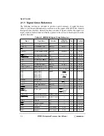
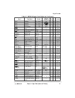
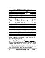
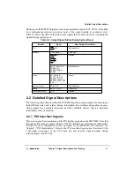
Detailed Signal Descriptions
2.2.2.5 Write Enable (WE)—Output
The write enable (WE) signal is an output on the MPC8240. For SDRAM, WE is part of
the SDRAM command encoding. See Section 6.2, “SDRAM Interface Operation,” for
more information. Following are the state meaning and timing comments for the WE output
signal for DRAM, ECO and Flash writes.
State Meaning
Asserted—Enables writing to DRAM, EDO, or Flash.
Negated—No DRAM, EDO, or Flash write operation is pending.
Timing Comments
Assertion—For DRAM, the MPC8240 asserts WE concurrent with
the column address and prior to CASn. For SDRAM, the MPC8240
asserts WE concurrent with SDCAS for write operations.
2.2.2.6 SDRAM Address (SDMA[11:0])—Output
The SDMA[11:0] signals carry 12 of the address bits for the memory interface. For
(S)DRAMs, they correspond to the row and column address bits.
State Meaning
Asserted/Negated—Contain different portions of the address
depending on the size of memory in use, the type of memory in use
(DRAM, SDRAM, ROM or Flash) and the phase of the transaction.
See Section 6.2.2, “SDRAM Address Multiplexing”, for a complete
description of the mapping of these signals in all cases.
Timing Comments
Assertion—For DRAM, the row address is considered valid on the
assertion of RASn, and the column address is valid on the assertion
of CASn. For SDRAM, the row address is valid on the rising edge of
SDRAM_CLK[0:3] clock signals when CSn is asserted and the
column address is valid on the rising edge of SDRAM_CLK[0:3]
when DQMn is asserted. For ROM and Flash, the address is valid
with the assertion of RCS0.
2.2.2.7 SDRAM Address 12 (SDMA12)—Output
The SDMA12 signal is similar to SDMA[11:0] in that it corresponds to different row or
column address bits, depending on the memory in use.
State Meaning
Asserted/Negated—See Section 6.2.2, “SDRAM Address
Multiplexing,” for a complete description of the mapping of this
signal in all cases.
Timing Comments
Assertion/Negation—The same as SDMA[11:0].
2.2.2.8 SDRAM Internal Bank Select 0–1 (SDBA0, SDBA1)—Output
The SDBA[0:1] signals are similar to SDMA[11:0] in that they correspond to different row
or column address bits, depending on the memory in use. However, they are only used for
the SDRAM interface. Note that SDBA1 is multiplexed with the SDMA12 signal.
Summary of Contents for MPC8240
Page 1: ...MPC8240UM D Rev 1 1 2001 MPC8240 Integrated Processor User s Manual ...
Page 38: ...xviii MPC8240 Integrated Processor User s Manual TABLES Table Number Title Page Number ...
Page 48: ...xlviii MPC8240 Integrated Processor User s Manual Acronyms and Abbreviations ...
Page 312: ...6 94 MPC8240 Integrated Processor User s Manual ROM Flash Interface Operation ...
Page 348: ...7 36 MPC8240 Integrated Processor User s Manual PCI Host and Agent Modes ...
Page 372: ...8 24 MPC8240 Integrated Processor User s Manual DMA Register Descriptions ...
Page 394: ...9 22 MPC8240 Integrated Processor User s Manual I2O Interface ...
Page 412: ...10 18 MPC8240 Integrated Processor User s Manual Programming Guidelines ...
Page 454: ...12 14 MPC8240 Integrated Processor User s Manual Internal Arbitration ...
Page 466: ...13 12 MPC8240 Integrated Processor User s Manual Exception Latencies ...
Page 516: ...16 14 Watchpoint Trigger Applications ...
Page 538: ...B 16 MPC8240 Integrated Processor User s Manual Setting the Endian Mode of Operation ...
Page 546: ...C 8 MPC8240 Integrated Processor User s Manual ...
Page 640: ...INDEX Index 16 MPC8240 Integrated Processor User s Manual ...


