Chapter 2. Signal Descriptions and Clocking
2-35
Clocking
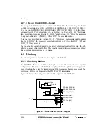
The sys_logic_clk signal may be set to a multiple of the PCI bus frequency as defined in the
MPC8240 Hardware Specification. To help reduce the amount of discrete logic required in
a system, the MPC8240 provides PCI clock fanout buffers. The MPC8240 also provides the
memory clock (SDRAM_CLKn) signals through a delay locked loop (DLL) that is running
at the same frequency as the internal system logic (sys_logic_clk).
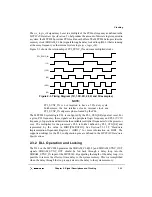
Figure 2-3 shows the relationship of PCI_SYNC_IN and some multiplied clocks.
)
Figure 2-3. Timing Diagram (1X, 1.5X, 2X, 2.5X, and 3X examples)
NOTE:
PCI_SYNC_IN is not required to have a 50% duty cycle.
Furthermore, the bus interface clocks, internal clock and
PCI_SYNC_IN edges are phase-locked by the PLL.
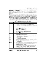
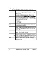
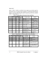
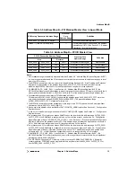
The MPC8240 system logic PLL is configured by the PLL_CFG[0:4] signals at reset. For
a given PCI frequency, these signals set the peripheral logic frequency and PLL (VCO)
frequency of operation and determine the available multiplier frequencies for the processor
core. The multiplier for the processor’s PLL is further defined by PLL_CFG[0:4] and
represented by the value in HID1[PLLRATIO]. See Section 5.3.1.2.2, “Hardware
Implementation-Dependent Register 1 (HID1),” for more information on HID1. The
supported settings for the PLL configuration pins are defined in the MPC8240 Hardware
Specifications.
2.3.2 DLL Operation and Locking
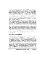
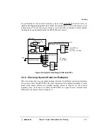
The DLL on the MPC8240 generates the SDRAM_CLK[0:3] and SDRAM_SYNC_OUT
signals. SDRAM_SYNC_OUT should be fed back through a delay loop into the
SDRAM_SYNC_IN input of the MPC8240. By adjusting the length of the delay loop, it is
possible to remove the effects of trace delay to the system memory. This is accomplished
when the delay through the loop is equivalent to the delay to the system memory.
PCI_SYNC_IN
(2X)
(3X)
(1.5X)
(1X)
(2.5X)
Summary of Contents for MPC8240
Page 1: ...MPC8240UM D Rev 1 1 2001 MPC8240 Integrated Processor User s Manual ...
Page 38: ...xviii MPC8240 Integrated Processor User s Manual TABLES Table Number Title Page Number ...
Page 48: ...xlviii MPC8240 Integrated Processor User s Manual Acronyms and Abbreviations ...
Page 312: ...6 94 MPC8240 Integrated Processor User s Manual ROM Flash Interface Operation ...
Page 348: ...7 36 MPC8240 Integrated Processor User s Manual PCI Host and Agent Modes ...
Page 372: ...8 24 MPC8240 Integrated Processor User s Manual DMA Register Descriptions ...
Page 394: ...9 22 MPC8240 Integrated Processor User s Manual I2O Interface ...
Page 412: ...10 18 MPC8240 Integrated Processor User s Manual Programming Guidelines ...
Page 454: ...12 14 MPC8240 Integrated Processor User s Manual Internal Arbitration ...
Page 466: ...13 12 MPC8240 Integrated Processor User s Manual Exception Latencies ...
Page 516: ...16 14 Watchpoint Trigger Applications ...
Page 538: ...B 16 MPC8240 Integrated Processor User s Manual Setting the Endian Mode of Operation ...
Page 546: ...C 8 MPC8240 Integrated Processor User s Manual ...
Page 640: ...INDEX Index 16 MPC8240 Integrated Processor User s Manual ...

