4-22
MPC8240 Integrated Processor User’s Manual
Embedded Utilities Memory Block Base Address Register—0x78
4.5 Embedded Utilities Memory Block Base Address
Register—0x78
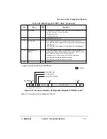
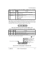
The embedded utilities memory block base address register (EUMBBAR), shown in
Table 4-19, controls the placement of the embedded utilities memory block (EUMB). See
Section 3.4, “Embedded Utilities Memory Block (EUMB).”
Table 4-18. CLK Driver Control Register Bit Definitions—0x74
Bit Name
Reset
Value
Description
15
addr<75>
—
x
Reserved
14
PCI_CLK0_DIS
0
This bit disables/enables the PCI_CLK0 output of MPC8420. A value of
one (0b1) disables the output. A value of zero (0b0) enables the output.
13
PCI_CLK1_DIS
0
This bit disables/enables the PCI_CLK1 output of MPC8420. A value of
one (0b1) disables the output. A value of zero (0b0) enables the output.
12
PCI_CLK2 _DIS
0
This bit disables/enables the PCI_CLK2 output of MPC8420. A value of
one (0b1) disables the output. A value of zero (0b0) enables the output.
11
PCI_CLK3_DIS
0
This bit disables/enables the PCI_CLK3 output of MPC8420. A value of
one (0b1) disables the output. A value of zero (0b0) enables the output.
10
PCI_CLK4_DIS
0
This bit disables/enables the PCI_CLK4 output of MPC8420. A value of
one (0b1) disables the output. A value of zero (0b0) enables the output.
9–8
—
00
Reserved
7
addr<74>
—
x
Reserved
6
SDRAM_CLK0_DIS
0
This bit disables/enables the SDRAM_CLK0 output of MPC8420. A
value of one (0b1) disables the output. A value of zero (0b0) enables
the output.
5
SDRAM_CLK1_DIS
0
This bit disables/enables the SDRAM_CLK1 output of MPC8420. A
value of one (0b1) disables the output. A value of zero (0b0) enables
the output.
4
SDRAM_CLK2_DIS
0
This bit disables/enables the SDRAM_CLK2 output of MPC8420. A
value of one (0b1) disables the output. A value of zero (0b0) enables
the output.
3
SDRAM_CLK3_DIS
0
This bit disables/enables the SDRAM_CLK3 output of MPC8420. A
value of one (0b1) disables the output. A value of zero (0b0) enables
the output.
2–0
—
000
Reserved
Summary of Contents for MPC8240
Page 1: ...MPC8240UM D Rev 1 1 2001 MPC8240 Integrated Processor User s Manual ...
Page 38: ...xviii MPC8240 Integrated Processor User s Manual TABLES Table Number Title Page Number ...
Page 48: ...xlviii MPC8240 Integrated Processor User s Manual Acronyms and Abbreviations ...
Page 312: ...6 94 MPC8240 Integrated Processor User s Manual ROM Flash Interface Operation ...
Page 348: ...7 36 MPC8240 Integrated Processor User s Manual PCI Host and Agent Modes ...
Page 372: ...8 24 MPC8240 Integrated Processor User s Manual DMA Register Descriptions ...
Page 394: ...9 22 MPC8240 Integrated Processor User s Manual I2O Interface ...
Page 412: ...10 18 MPC8240 Integrated Processor User s Manual Programming Guidelines ...
Page 454: ...12 14 MPC8240 Integrated Processor User s Manual Internal Arbitration ...
Page 466: ...13 12 MPC8240 Integrated Processor User s Manual Exception Latencies ...
Page 516: ...16 14 Watchpoint Trigger Applications ...
Page 538: ...B 16 MPC8240 Integrated Processor User s Manual Setting the Endian Mode of Operation ...
Page 546: ...C 8 MPC8240 Integrated Processor User s Manual ...
Page 640: ...INDEX Index 16 MPC8240 Integrated Processor User s Manual ...


