
Chapter 4. Configuration Registers
4-43
Memory Control Configuration Registers
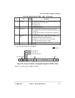
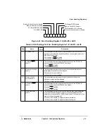
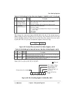
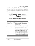
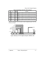
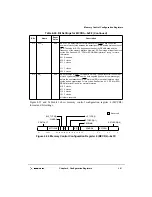
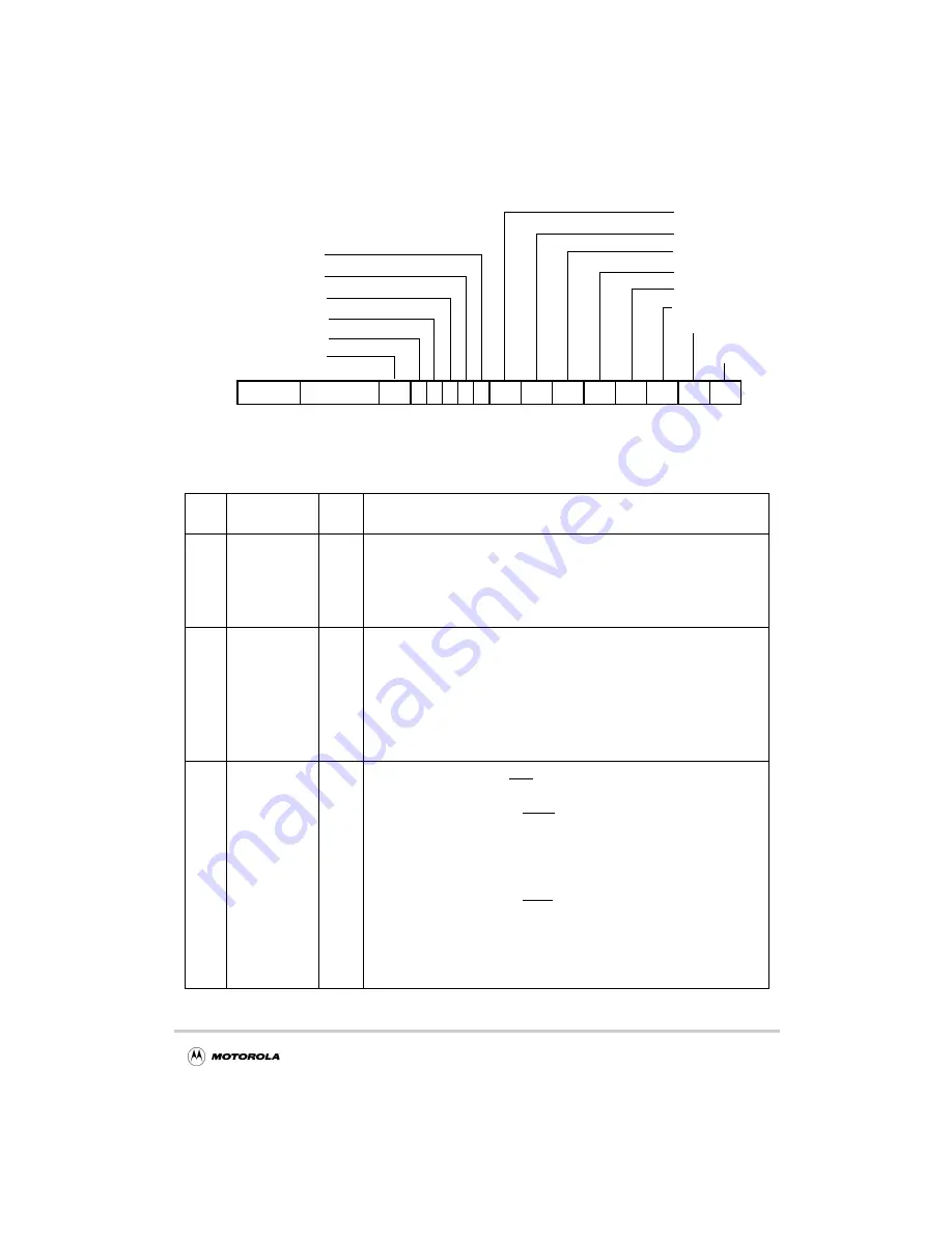
Figure 4-29. Memory Control Configuration Register 1 (MCCR1)—0xF0
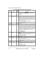
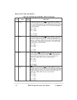
Table 4-38. Bit Settings for MCCR1—0xF0
Bits
Name
Reset
Value
Description
31–28
ROMNAL
All 1s
For burst-mode ROM and Flash reads, ROMNAL controls the next access time.
The maximum value is 0b1111 (15). The actual cycle count is three cycles more
than the binary value of ROMNAL.
For Flash writes, ROMNAL measures the write pulse recovery (high) time. The
maximum value is 0b1111 (15). The actual cycle count is four cycles more than
the binary value of ROMNAL.
27–23
ROMFAL
All 1s
For nonburst ROM and Flash reads, ROMFAL controls the access time. For
burst-mode ROMs, ROMFAL controls the first access time. The maximum value
is 0b11111 (31). For the 64-bit and 32-bit configurations, the actual cycle count
is three cycles more than the binary value of ROMFAL. For the 8-bit
configuration, the actual cycle count is two cycles more than the binary value of
ROMFAL.
For Flash writes, ROMFAL measures the write pulse low time. The maximum
value is 0b11111 (31). The actual cycle count is two cycles more than the binary
value of ROMFAL.
22–21
DBUS_SIZ[0–1]
xx
Read-only. This field indicates the state of the ROM bank 0 data path width
configuration signals [DL[0], FOE] at reset as follows.
For ROM/Flash chip select #0 (RCSO),
00 32-bit data bus.
x1 8-bit data bus.
10 64-bit data bus.
For ROM/Flash chip select #1 (RCS1) and (S)DRAM,
0x 32-bit data bus.
For FPM/EDO systems only, (RAM_TYPE=1).
1x 64-bit data bus.
ROMNAL
ROMFAL
31
28 27
23 22 21 20 19 18 17 16 15 14 13 12 11 10
9
8
7
6
5
4
3
2
1
0
MEMGO
DBUS_SIZ[0–1]
BURST
PCKEN
SREN
Bank 7 Row
RAM_TYPE
Bank 0
Row
Bank 3 Row
Bank 2 Row
Bank 1 Row
Bank 6 Row
Bank 5 Row
Bank 4 Row
Summary of Contents for MPC8240
Page 1: ...MPC8240UM D Rev 1 1 2001 MPC8240 Integrated Processor User s Manual ...
Page 38: ...xviii MPC8240 Integrated Processor User s Manual TABLES Table Number Title Page Number ...
Page 48: ...xlviii MPC8240 Integrated Processor User s Manual Acronyms and Abbreviations ...
Page 312: ...6 94 MPC8240 Integrated Processor User s Manual ROM Flash Interface Operation ...
Page 348: ...7 36 MPC8240 Integrated Processor User s Manual PCI Host and Agent Modes ...
Page 372: ...8 24 MPC8240 Integrated Processor User s Manual DMA Register Descriptions ...
Page 394: ...9 22 MPC8240 Integrated Processor User s Manual I2O Interface ...
Page 412: ...10 18 MPC8240 Integrated Processor User s Manual Programming Guidelines ...
Page 454: ...12 14 MPC8240 Integrated Processor User s Manual Internal Arbitration ...
Page 466: ...13 12 MPC8240 Integrated Processor User s Manual Exception Latencies ...
Page 516: ...16 14 Watchpoint Trigger Applications ...
Page 538: ...B 16 MPC8240 Integrated Processor User s Manual Setting the Endian Mode of Operation ...
Page 546: ...C 8 MPC8240 Integrated Processor User s Manual ...
Page 640: ...INDEX Index 16 MPC8240 Integrated Processor User s Manual ...


