4-48
MPC8240 Integrated Processor User’s Manual
Memory Control Configuration Registers
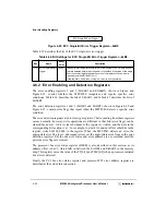
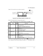
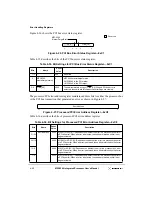
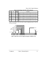
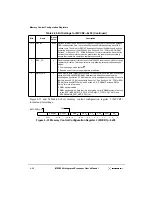
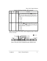
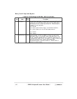
Figure 4-31 and Table 4-40 show memory control configuration register 3 (MCCR3)
format and bit settings.
Figure 4-31. Memory Control Configuration Register 3 (MCCR3)—0xF8
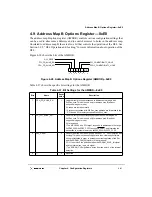
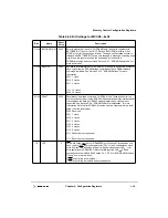
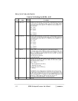
15–2
REFINT
All 0s
Refresh interval. These bits directly represent the number of clock cycles between
CBR refresh cycles. One row is refreshed in each RAM bank during each CBR
refresh cycle. The value for REFINT depends on the specific RAMs used and the
operating frequency of the MPC8240. See Section 6.3.10, “FPM or EDO DRAM
Refresh,” or Section 6.2.12, “SDRAM Refresh,” for more information. Note that the
period of the refresh interval must be greater than the read/write access time to
ensure that read/write operations complete successfully.
1
RSV_PG
0
Reserve page register. If this bit is set, the MPC8240 reserves one of the four page
registers at all times. This is equivalent to only allowing three simultaneous open
pages.
0 Four open page mode (default)
1 Reserve one of the four page registers at all times
0
RMW_PAR
0
Read-modify-write (RMW) parity enable. This bit controls how the MPC8240 writes
parity bits to DRAM/EDO/SDRAM. Note that this bit does not enable parity
checking and generation. PCKEN must be set to enable parity checking. Also note
that this bit and ECC_EN cannot both be set to 1. See Section 6.3.8, “FPM or EDO
DRAM Parity and RMW Parity,” and Section 6.2.9, “SDRAM Parity and RMW
Parity,” for more information.
0 RMW parity disabled
1 RMW parity enabled. Note that this bit must be set for SDRAM systems that use
in-line ECC (MCCR2[ECC_EN] = 0, MCCR4[BUF_TYPE[0–1]] = 0b10, and
MCCR2[INLINE_PAR_NOT_ECC]] = 0).
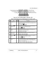
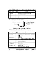
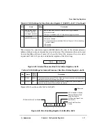
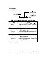
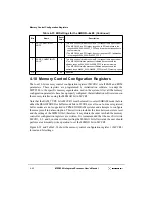
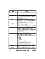
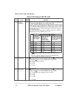
Table 4-39. Bit Settings for MCCR2—0xF4 (Continued)
Bits
Name
Reset
Value
Description
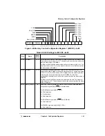
REFREC
RDLAT
RAS
6P
CAS
5
CP
4
CAS
3
RCD
2
RP
1
31
28 27
24 23
20 19 18
15 14
12 11
9
8
6
5
3
2
0
BSTOPRE[2–5]
CPX
Summary of Contents for MPC8240
Page 1: ...MPC8240UM D Rev 1 1 2001 MPC8240 Integrated Processor User s Manual ...
Page 38: ...xviii MPC8240 Integrated Processor User s Manual TABLES Table Number Title Page Number ...
Page 48: ...xlviii MPC8240 Integrated Processor User s Manual Acronyms and Abbreviations ...
Page 312: ...6 94 MPC8240 Integrated Processor User s Manual ROM Flash Interface Operation ...
Page 348: ...7 36 MPC8240 Integrated Processor User s Manual PCI Host and Agent Modes ...
Page 372: ...8 24 MPC8240 Integrated Processor User s Manual DMA Register Descriptions ...
Page 394: ...9 22 MPC8240 Integrated Processor User s Manual I2O Interface ...
Page 412: ...10 18 MPC8240 Integrated Processor User s Manual Programming Guidelines ...
Page 454: ...12 14 MPC8240 Integrated Processor User s Manual Internal Arbitration ...
Page 466: ...13 12 MPC8240 Integrated Processor User s Manual Exception Latencies ...
Page 516: ...16 14 Watchpoint Trigger Applications ...
Page 538: ...B 16 MPC8240 Integrated Processor User s Manual Setting the Endian Mode of Operation ...
Page 546: ...C 8 MPC8240 Integrated Processor User s Manual ...
Page 640: ...INDEX Index 16 MPC8240 Integrated Processor User s Manual ...

