Chapter 5. PowerPC Processor Core
5-5
PowerPC Processor Core Features
•
Facilities for enhanced system performance
— A 32- or 64-bit split-transaction internal data bus interface to the peripheral logic
bus with bursting
— Support for one-level address pipelining and out-of-order bus transactions
— Hardware support for misaligned little-endian accesses
— Cofigurable processor bus frequency multipliers as defined in the MPC8240
Integrated Processor Hardware Specifications.
•
Integrated power management
— Three power-saving modes: doze, nap, and sleep
— Automatic dynamic power reduction when internal functional units are idle
•
Deterministic behavior and debug features
— On-chip cache locking options for the instruction and data caches (1–3 ways or
the entire cache contents can be locked)
— In-system testability and debugging features through JTAG and boundary-scan
capability
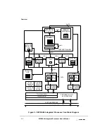
Figure 5-1 shows how the execution units (IU, BPU, FPU, LSU, and SRU) operate
independently and in parallel. Note that this is a conceptual diagram and does not attempt
to show how these features are physically implemented on the chip.
5.2.1 Instruction Unit
As shown in Figure 5-1, the instruction unit, which contains a fetch unit, instruction queue,
dispatch unit, and the BPU, provides centralized control of instruction flow to the execution
units. The instruction unit determines the address of the next instruction to be fetched based
on information from the sequential fetcher and from the BPU.
The instruction unit fetches the instructions from the instruction cache into the instruction
queue. The BPU extracts branch instructions from the fetcher and uses static branch
prediction on unresolved conditional branches to allow the instruction unit to fetch
instructions from a predicted target instruction stream while a conditional branch is
evaluated. The BPU folds out branch instructions for unconditional branches or conditional
branches unaffected by instructions in progress in the execution pipeline.
Instructions issued beyond a predicted branch do not complete execution until the branch
is resolved, preserving the programming model of sequential execution. If any of these
instructions are to be executed in the BPU, they are decoded but not issued. Instructions to
be executed by the IU, FPU, LSU, and SRU are issued and allowed to complete up to the
register write-back stage. Write-back is allowed when a correctly predicted branch is
resolved, and instruction execution continues without interruption on the predicted path. If
branch prediction is incorrect, the instruction unit flushes all predicted path instructions,
and instructions are issued from the correct path.
Summary of Contents for MPC8240
Page 1: ...MPC8240UM D Rev 1 1 2001 MPC8240 Integrated Processor User s Manual ...
Page 38: ...xviii MPC8240 Integrated Processor User s Manual TABLES Table Number Title Page Number ...
Page 48: ...xlviii MPC8240 Integrated Processor User s Manual Acronyms and Abbreviations ...
Page 312: ...6 94 MPC8240 Integrated Processor User s Manual ROM Flash Interface Operation ...
Page 348: ...7 36 MPC8240 Integrated Processor User s Manual PCI Host and Agent Modes ...
Page 372: ...8 24 MPC8240 Integrated Processor User s Manual DMA Register Descriptions ...
Page 394: ...9 22 MPC8240 Integrated Processor User s Manual I2O Interface ...
Page 412: ...10 18 MPC8240 Integrated Processor User s Manual Programming Guidelines ...
Page 454: ...12 14 MPC8240 Integrated Processor User s Manual Internal Arbitration ...
Page 466: ...13 12 MPC8240 Integrated Processor User s Manual Exception Latencies ...
Page 516: ...16 14 Watchpoint Trigger Applications ...
Page 538: ...B 16 MPC8240 Integrated Processor User s Manual Setting the Endian Mode of Operation ...
Page 546: ...C 8 MPC8240 Integrated Processor User s Manual ...
Page 640: ...INDEX Index 16 MPC8240 Integrated Processor User s Manual ...

