6-48
MPC8240 Integrated Processor User’s Manual
FPM or EDO DRAM Interface Operation
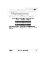
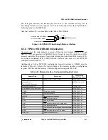
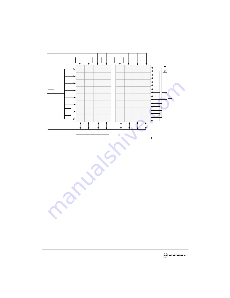
Figure 6-31. DRAM Memory Organization
6.3.1 Supported FPM or EDO DRAM Organizations
It is not necessary to use identical memory devices in each memory bank; individual
memory banks may be of differing sizes but not of different type (SDRAM). The MPC8240
can be configured to provide 9–13 row bits to a particular bank, and 7–12 column bits.
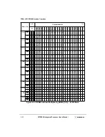
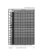
Table 6-17 summarizes the DRAM configurations supported by the MPC8240. This table
is not exhaustive, although it covers most available DRAMs. The largest DRAM that can
be supported is limited to 24 total address bits.
The MPC8240 can be configured at system start-up by using a memory-polling algorithm
or hard code in a boot ROM, to map correctly the size of each bank in memory. The
MPC8240 uses its bank map to assert the appropriate RAS[0:7] signals for memory
accesses according to the provided bank depths.
System software must also configure MCCR1 register in the MPC8240 at system start-up
to appropriately multiplex the row and column address bits for each bank for the devices
being used as shown in Table 6-17. Any unused banks should have their starting and ending
addresses programmed out of the range of memory banks in use. Otherwise memory may
become corrupted in the overlapping address range. Any unused banks should have their
starting and ending addresses programmed out of the range of memory banks in use.
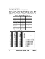
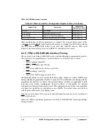
Table 6-16 shows the unsupported multiplexed row and column address bit configurations
in the 32- and 64-bit data bus mode. They result in non-contiguous address spaces.
CAS
[7]
RAS[0]
RAS[1]
RAS[2]
RAS[3]
RAS[4]
RAS[6]
RAS[7]
RAS[5]
RAS[0:7]
CAS[0:7]
SDBA[1:0]
WE
8 bits
256K –16M bits
8 bits
8 bits
8 bits
8 bits
8 bits
8 bits
8 bits
MDH[0:31], MDL[0:31]
BANK0
BANK7
CAS
[6]
CAS
[5]
CAS
[4]
CAS
[3]
CAS
[2]
CAS
[1]
CAS
[0]
32-bit Mode
64-bit Mode
MDH(0:31)
MDL(0:31)
SDMA[12:0]
Summary of Contents for MPC8240
Page 1: ...MPC8240UM D Rev 1 1 2001 MPC8240 Integrated Processor User s Manual ...
Page 38: ...xviii MPC8240 Integrated Processor User s Manual TABLES Table Number Title Page Number ...
Page 48: ...xlviii MPC8240 Integrated Processor User s Manual Acronyms and Abbreviations ...
Page 312: ...6 94 MPC8240 Integrated Processor User s Manual ROM Flash Interface Operation ...
Page 348: ...7 36 MPC8240 Integrated Processor User s Manual PCI Host and Agent Modes ...
Page 372: ...8 24 MPC8240 Integrated Processor User s Manual DMA Register Descriptions ...
Page 394: ...9 22 MPC8240 Integrated Processor User s Manual I2O Interface ...
Page 412: ...10 18 MPC8240 Integrated Processor User s Manual Programming Guidelines ...
Page 454: ...12 14 MPC8240 Integrated Processor User s Manual Internal Arbitration ...
Page 466: ...13 12 MPC8240 Integrated Processor User s Manual Exception Latencies ...
Page 516: ...16 14 Watchpoint Trigger Applications ...
Page 538: ...B 16 MPC8240 Integrated Processor User s Manual Setting the Endian Mode of Operation ...
Page 546: ...C 8 MPC8240 Integrated Processor User s Manual ...
Page 640: ...INDEX Index 16 MPC8240 Integrated Processor User s Manual ...


