6-64
MPC8240 Integrated Processor User’s Manual
FPM or EDO DRAM Interface Operation
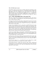
The MPC8240 supports concurrent ECC for the FPM or EDO data path and parity for the
processor core data path. ECC and parity may be independently enabled or disabled. The
eight signals used for ECC (PAR[0:7]) are also used for processor core parity. The
MPC8240 checks ECC on all memory reads (provided ECC_EN = 1). The MPC8240
supports a read-modify-write mode similar to the RMW parity mode described above for
writes smaller than double word writes. The MPC8240 does not support ECC when in
32-bit data path mode (ECC_EN = 0).
6.3.9.1 FPM or EDO DRAM Interface Timing with ECC
When ECC is enabled, the time required to check and generate the ECC codes increases
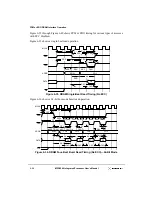
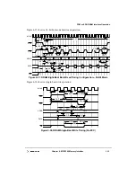
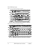
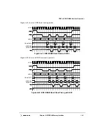
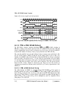
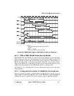
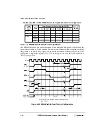
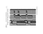
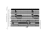
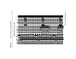
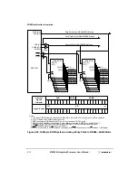
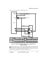
access latency. Figure 6-39 through Figure 6-40 shows FPM or EDO timings for various
types of accesses with ECC enabled.
For processor burst reads from system memory, checking the ECC codes for errors requires
two additional clock cycles for the first data returned and at least four clock cycles for
subsequent beats. These requirements do not depend on the buffer type or whether FPM or
EDO is used for system memory.
For processor core single-beat writes to system memory, the MPC8240 latches the data,
performs a double-word read from system memory (checking and correcting any ECC
errors), and merges the write data from the processor with the data read from memory. The
MPC8240 then generates a new ECC code for the merged double word and writes the data
and ECC code to memory. This read-modify-write process adds six clock cycles to a
single-beat write operation. If page mode retention is enabled (PGMAX > 0), the MPC8240
keeps the memory in page mode for the read-modify-write sequence.
For processor core burst writes to system memory, the MPC8240 latches the data in the
internal copyback buffer and flushes the buffer to memory at the earliest opportunity. The
MPC8240 generates the ECC codes when the flush occurs. Note that the MPC8240 does
not check the data being overwritten in memory.
For PCI writes to system memory with ECC enabled, the MPC8240 latches the data in the
internal PCI to memory write buffer (PCMWB). If the PCI master writes complete double
words to system memory, the MPC8240 generates the ECC codes when the PCMWB is
flushed to memory.
If the PCI master writes 32-, 16-, or 8-bit data that cannot be gathered into a complete
double word in the PCMWB, a read-modify-write operation is required.
The MPC8240 performs a double-word read from system memory (checking and
correcting any ECC errors), then merges the write data from the PCI master with the data
read from memory, generates a new ECC code for the merged double word, and writes the
data and ECC code to memory.
Summary of Contents for MPC8240
Page 1: ...MPC8240UM D Rev 1 1 2001 MPC8240 Integrated Processor User s Manual ...
Page 38: ...xviii MPC8240 Integrated Processor User s Manual TABLES Table Number Title Page Number ...
Page 48: ...xlviii MPC8240 Integrated Processor User s Manual Acronyms and Abbreviations ...
Page 312: ...6 94 MPC8240 Integrated Processor User s Manual ROM Flash Interface Operation ...
Page 348: ...7 36 MPC8240 Integrated Processor User s Manual PCI Host and Agent Modes ...
Page 372: ...8 24 MPC8240 Integrated Processor User s Manual DMA Register Descriptions ...
Page 394: ...9 22 MPC8240 Integrated Processor User s Manual I2O Interface ...
Page 412: ...10 18 MPC8240 Integrated Processor User s Manual Programming Guidelines ...
Page 454: ...12 14 MPC8240 Integrated Processor User s Manual Internal Arbitration ...
Page 466: ...13 12 MPC8240 Integrated Processor User s Manual Exception Latencies ...
Page 516: ...16 14 Watchpoint Trigger Applications ...
Page 538: ...B 16 MPC8240 Integrated Processor User s Manual Setting the Endian Mode of Operation ...
Page 546: ...C 8 MPC8240 Integrated Processor User s Manual ...
Page 640: ...INDEX Index 16 MPC8240 Integrated Processor User s Manual ...


