6-76
MPC8240 Integrated Processor User’s Manual
ROM/Flash Interface Operation
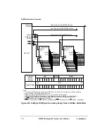
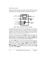
Note that the 8-bit data path requires external decode logic to select between the two
devices. Also note that the 21st ROM/Flash address bit (SDMA12/SDBA1) is supported
only for bank 0 using the 8-bit data path and for both banks using the 32-bit data path.
The extra address bit allows for up to 2 Mbytes of ROM/Flash space in bank 0 for the 8-bit
data path configuration and up to 16 Mbytes of ROM/Flash space using both banks for the
32-bit data path configuration. For the 64-bit data path, 20 address bits allow for up to 8
Mbytes per bank for a total of 16 Mbytes using both banks. See Table 6-26.
When 64-bit SDRAM/DRAM is selected (MDL[0] =1), ROM/Flash only can be 8- or
64-bit (no 32-bit ROM/Flash).
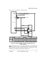
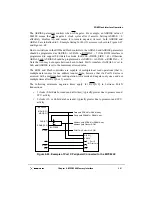
For systems using the 8-bit interface to bank 0, the ROM/Flash device must be connected
to the most-significant byte lane of the data bus MDH[0:7]. The MPC8240 performs byte-
lane alignment for single-byte reads from ROM/Flash memory. The MPC8240 can also
perform byte gathering for up to 8 bytes for ROM/Flash read operations. The data bytes are
gathered and aligned within the MPC8240, and then forwarded to the local processor.
The 16-Mbyte ROM/Flash space is subdivided into two 8-Mbyte banks. Bank 0 (selected
by RCS0) is addressed from 0xFF80_0000 to 0xFFFF_FFFF. Bank 1 (selected by RCS1)
is addressed from 0xFF00_0000 to 0xFF7F_FFFF. Implementations that require less than
16 Mbytes may allocate the required ROM/Flash to one or both banks.
For example, an implementation that requires only 4 Mbytes of ROM/Flash could locate
the ROM/Flash entirely within bank 0 at addresses 0xFFC0_0000–0xFFFF_FFFF.
Alternately, the ROM/Flash could be split across both banks with 2 Mbytes in bank 0 at
0xFFE0_0000–0xFFFF_FFFF and 2 Mbytes in bank 1 at 0xFF60_0000–0xFF7F_FFFF.
Any system ROM space that is not physically implemented within a bank is aliased to any
physical device within that bank.
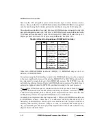
Table 6-26. Reset Configurations of ROM/Flash Controller
MDL[0]
FOE
Bank 0
Bank 1
0
0
32-bit interface
21 address bits
8 Meg space
32-bit interface
21 address bits
8 Meg space
1
0
64-bit interface
20 address bits
8 Meg space
64-bit interface
20 address bits
8 Meg space
0
1
8-bit interface
21 address bits
2 Meg space
32-bit interface
21 address bits
8 Meg space
1
1
8-bit interface
21 address bits
2 Meg space
64-bit interface
20 address bits
8 Meg space
Summary of Contents for MPC8240
Page 1: ...MPC8240UM D Rev 1 1 2001 MPC8240 Integrated Processor User s Manual ...
Page 38: ...xviii MPC8240 Integrated Processor User s Manual TABLES Table Number Title Page Number ...
Page 48: ...xlviii MPC8240 Integrated Processor User s Manual Acronyms and Abbreviations ...
Page 312: ...6 94 MPC8240 Integrated Processor User s Manual ROM Flash Interface Operation ...
Page 348: ...7 36 MPC8240 Integrated Processor User s Manual PCI Host and Agent Modes ...
Page 372: ...8 24 MPC8240 Integrated Processor User s Manual DMA Register Descriptions ...
Page 394: ...9 22 MPC8240 Integrated Processor User s Manual I2O Interface ...
Page 412: ...10 18 MPC8240 Integrated Processor User s Manual Programming Guidelines ...
Page 454: ...12 14 MPC8240 Integrated Processor User s Manual Internal Arbitration ...
Page 466: ...13 12 MPC8240 Integrated Processor User s Manual Exception Latencies ...
Page 516: ...16 14 Watchpoint Trigger Applications ...
Page 538: ...B 16 MPC8240 Integrated Processor User s Manual Setting the Endian Mode of Operation ...
Page 546: ...C 8 MPC8240 Integrated Processor User s Manual ...
Page 640: ...INDEX Index 16 MPC8240 Integrated Processor User s Manual ...

