Chapter 6. MPC8240 Memory Interface
6-83
ROM/Flash Interface Operation
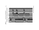
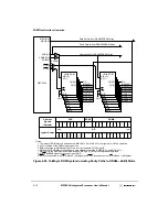
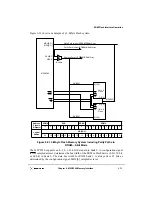
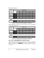
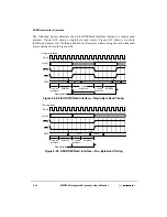
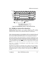
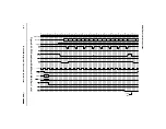
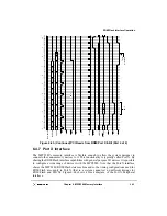
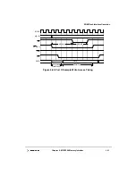
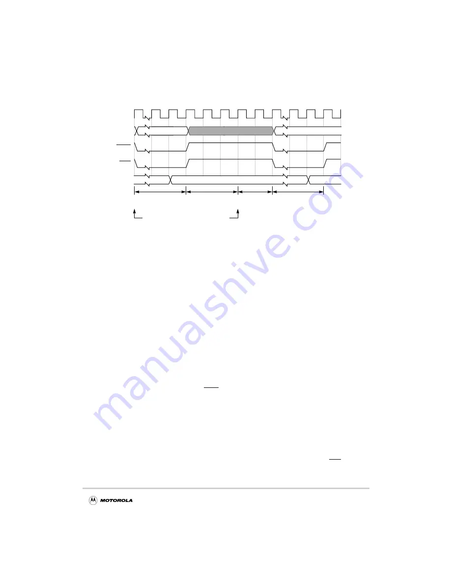
Figure 6-60. 8-Bit ROM/Flash Interface—Cache-Line Read Timing
6.4.4 ROM/Flash Interface Write Operations
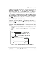
PICR1[FLASH_WR_EN] must be set for write operations to Flash memory.
FLASH_WR_EN controls whether write operations to Flash memory are allowed.
FLASH_WR_EN is cleared at reset to disable write operations to Flash memory.
Writes to Flash can be locked out by setting PCIR2 [FLASH_WR_LOCKOUT]. When this
bit is set, the MPC8240 disables writing to Flash memory, even if FLASH_WR_EN is set.
Once set, the FLASH_WR_LOCKOUT parameter can be cleared only by a hard reset.
If the system attempts to write to read-only devices in a bank, bus contention may occur.
This is because the write data is driven onto the data bus when the read-only device is also
trying to drive its data onto the data bus. This situation can be avoided by disabling writes
to the system ROM space using FLASH_WR_EN or FLASH_WR_LOCKOUT or by
connecting the Flash output enable (FOE) signal to the output enable on the read-only
device.
System logic is responsible for multiplexing the required high voltages to the Flash
memory for write operations.
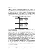
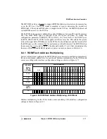
The MPC8240 accommodates only single-beat writes to Flash memory. If an attempt is
made to write to Flash with a data size other than the full data path size, the MPC8240 does
not report an error. Thus, if software is writing to Flash, the write operations should be sized
to the data path width (8, 32 or 64 bits) since there is only a single write enable (WE) strobe
available.
MCLK
A[0:19]1
RCSn
DATA
New fetch begins
FOE
Burst read
2 cycles
3 cycles
Repeated 4 times for complete burst
(2 +ROMFAL)
2 In-line mode adds an additional clock
1 Address toggles for each of 8 single-byte addresses
ROMFAL (ROM first access latency) = 0–31 cycles
x 8 cycles
(constant)2
between bursts
(minimum)2
Summary of Contents for MPC8240
Page 1: ...MPC8240UM D Rev 1 1 2001 MPC8240 Integrated Processor User s Manual ...
Page 38: ...xviii MPC8240 Integrated Processor User s Manual TABLES Table Number Title Page Number ...
Page 48: ...xlviii MPC8240 Integrated Processor User s Manual Acronyms and Abbreviations ...
Page 312: ...6 94 MPC8240 Integrated Processor User s Manual ROM Flash Interface Operation ...
Page 348: ...7 36 MPC8240 Integrated Processor User s Manual PCI Host and Agent Modes ...
Page 372: ...8 24 MPC8240 Integrated Processor User s Manual DMA Register Descriptions ...
Page 394: ...9 22 MPC8240 Integrated Processor User s Manual I2O Interface ...
Page 412: ...10 18 MPC8240 Integrated Processor User s Manual Programming Guidelines ...
Page 454: ...12 14 MPC8240 Integrated Processor User s Manual Internal Arbitration ...
Page 466: ...13 12 MPC8240 Integrated Processor User s Manual Exception Latencies ...
Page 516: ...16 14 Watchpoint Trigger Applications ...
Page 538: ...B 16 MPC8240 Integrated Processor User s Manual Setting the Endian Mode of Operation ...
Page 546: ...C 8 MPC8240 Integrated Processor User s Manual ...
Page 640: ...INDEX Index 16 MPC8240 Integrated Processor User s Manual ...


