Chapter 6. MPC8240 Memory Interface
6-91
ROM/Flash Interface Operation
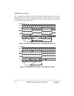
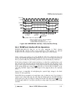
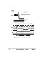
The ASRISE parameter controls when AS negates. For example, an ASRISE value of
0b0100 means that AS negates 4 clock cycles after it asserts. Setting ASRISE = 0
effectively disables AS and causes it to remain negated. At reset, both ASRISE and
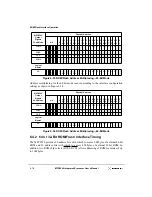
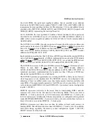
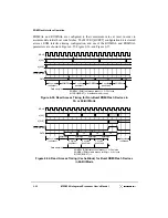
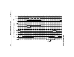
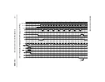
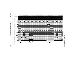
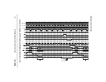
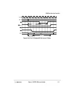
ASFALL are initialized to 0. Example timing for Port X accesses is shown in Figure 6-67
and Figure 6-68.
Due to restrictions in the ROM and Flash controllers, the ASFALL and ASRISE parameters
should be programmed as ASFALL
≤
7 if the ROM interface is
programmed to support 8-bit data bus mode for RCS0, (DBUS_SIZE = x1). Otherwise
ASFALL and ASRISE should be programmed as ASFALL
≤
4.
Note that AS may not negate between back-to-back Port X transfers if ASFALL is set to
0x0, and ASRISE is set to the maximum allowed value.
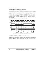
The ROM and Flash controllers are capable of multiple-beat read operations (that is,
multiple data tenures for one address tenure). Note, however, that if a Port X device is
accessed with a multiple-beat read operation, AS asserts and negates only once and not
multiple times after RCS[0 or 1] asserts.
The following minimum negation times apply for RCS[0–1] in between Port X
transactions:
•
5 clocks (8-bit data bus reads and all writes); typically greater due to processor and
CCU activity
•
2 clocks (32- or 64-bit data bus reads); typically greater due to processor and CCU
activity
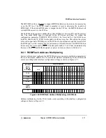
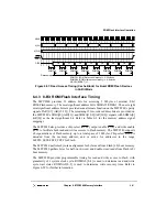
Figure 6-65. Example of Port X Peripheral Connected to the MPC8240
ROM Chip Select 0 to ROM
Data path SDRAM or DRAM Array
Address path SDRAM or DRAM Array
Parity path SDRAM or DRAM Array
Address path Flash or ROM
RCS0
WE
RCS1
MPC8240
SDMA[12:0]
PAR[0:7]
BUFFERS
MDH[0:31]
MDL[0:31]
Port X
I/O Device (s)
AS
CE
WE
A0:A18
AS
D[0:63]
Summary of Contents for MPC8240
Page 1: ...MPC8240UM D Rev 1 1 2001 MPC8240 Integrated Processor User s Manual ...
Page 38: ...xviii MPC8240 Integrated Processor User s Manual TABLES Table Number Title Page Number ...
Page 48: ...xlviii MPC8240 Integrated Processor User s Manual Acronyms and Abbreviations ...
Page 312: ...6 94 MPC8240 Integrated Processor User s Manual ROM Flash Interface Operation ...
Page 348: ...7 36 MPC8240 Integrated Processor User s Manual PCI Host and Agent Modes ...
Page 372: ...8 24 MPC8240 Integrated Processor User s Manual DMA Register Descriptions ...
Page 394: ...9 22 MPC8240 Integrated Processor User s Manual I2O Interface ...
Page 412: ...10 18 MPC8240 Integrated Processor User s Manual Programming Guidelines ...
Page 454: ...12 14 MPC8240 Integrated Processor User s Manual Internal Arbitration ...
Page 466: ...13 12 MPC8240 Integrated Processor User s Manual Exception Latencies ...
Page 516: ...16 14 Watchpoint Trigger Applications ...
Page 538: ...B 16 MPC8240 Integrated Processor User s Manual Setting the Endian Mode of Operation ...
Page 546: ...C 8 MPC8240 Integrated Processor User s Manual ...
Page 640: ...INDEX Index 16 MPC8240 Integrated Processor User s Manual ...

