Chapter 7. PCI Bus Interface
7-13
PCI Bus Protocol
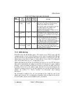
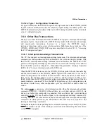
7.3.3.3 Configuration Space Addressing
PCI supports two types of configuration accesses which use different formats for the
AD[31:0] signals during the address phase. The two low-order bits of the address indicate
the format used for the configuration address phase—type 0 (AD[1:0] = 0b00) or type 1
(AD[1:0] = 0b01). Both address formats identify a specific device and a specific
configuration register for that device. See Section 7.4.5, “Configuration Cycles,” for
descriptions of the two formats.
7.3.4 Device Selection
The DEVSEL signal is driven by the target of the current transaction. DEVSEL indicates
to the other devices on the PCI bus that the target has decoded the address and claimed the
transaction. DEVSEL may be driven one, two, or three clock cycles (fast, medium, or slow
device select timing) following the address phase. Device select timing is encoded into the
device’s PCI status register. If no agent asserts DEVSEL within three clock cycles of
FRAME, the agent responsible for subtractive decoding may claim the transaction by
asserting DEVSEL.
A target must assert DEVSEL (claim the transaction) before or coincident with any other
target response (assert its TRDY, STOP, or data signals). In all cases except target-abort,
once a target asserts DEVSEL, it must not negate DEVSEL until FRAME is negated (with
IRDY asserted) and the last data phase has completed. For normal termination, negation of
DEVSEL coincides with the negation of TRDY or STOP.
If the first access maps into a target’s address range, that target asserts DEVSEL to claim
the access. However, if the initiator attempts to continue the burst access across the resource
boundary, then the target must issue a target disconnect.
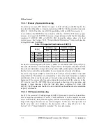
The MPC8240 is hardwired for fast device select timing (PCI status register[10–9] = 0b00).
Therefore, when the MPC8240 is the target of a transaction (local memory access or
configuration register access in agent mode), it asserts DEVSEL one clock cycle following
the address phase.
As an initiator, if the MPC8240 does not detect the assertion of DEVSEL within four clock
cycles after the address phase (that is, five clock cycles after it asserts FRAME), it
terminates the transaction with a master-abort termination; see Section
“Master-Initiated Termination.”
7.3.5 Byte Alignment
The byte enable signals of the PCI bus (C/BE[3:0], during a data phase) are used to
determine which byte lanes carry meaningful data. The byte enable signals may enable
different bytes for each of the data phases. The byte enables are valid on the edge of the
clock that starts each data phase and stay valid for the entire data phase. Note that parity is
calculated for all bytes regardless of the state of the byte enable signals. See Section 7.6.1,
“PCI Parity,” for more information.
Summary of Contents for MPC8240
Page 1: ...MPC8240UM D Rev 1 1 2001 MPC8240 Integrated Processor User s Manual ...
Page 38: ...xviii MPC8240 Integrated Processor User s Manual TABLES Table Number Title Page Number ...
Page 48: ...xlviii MPC8240 Integrated Processor User s Manual Acronyms and Abbreviations ...
Page 312: ...6 94 MPC8240 Integrated Processor User s Manual ROM Flash Interface Operation ...
Page 348: ...7 36 MPC8240 Integrated Processor User s Manual PCI Host and Agent Modes ...
Page 372: ...8 24 MPC8240 Integrated Processor User s Manual DMA Register Descriptions ...
Page 394: ...9 22 MPC8240 Integrated Processor User s Manual I2O Interface ...
Page 412: ...10 18 MPC8240 Integrated Processor User s Manual Programming Guidelines ...
Page 454: ...12 14 MPC8240 Integrated Processor User s Manual Internal Arbitration ...
Page 466: ...13 12 MPC8240 Integrated Processor User s Manual Exception Latencies ...
Page 516: ...16 14 Watchpoint Trigger Applications ...
Page 538: ...B 16 MPC8240 Integrated Processor User s Manual Setting the Endian Mode of Operation ...
Page 546: ...C 8 MPC8240 Integrated Processor User s Manual ...
Page 640: ...INDEX Index 16 MPC8240 Integrated Processor User s Manual ...

