11-4
MPC8240 Integrated Processor User’s Manual
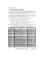
EPIC Register Summary
11.2 EPIC Register Summary
The EPIC register map occupies a 256-Kbyte range of the embedded utilities memory
block (EUMB). For further details, see Section 3.4, “Embedded Utilities Memory Block
(EUMB).” If an access is attempted to an undefined portion of the map, the device returns
0x0000_0000 as its value on reads and does nothing on writes.
All EPIC registers are 32 bits wide and reside on 128-bit address boundaries. All addresses
mentioned in this chapter are offsets from the EUMBBAR located at 0x78; see Section 4.5,
“Embedded Utilities Memory Block Base Address Register—0x78.”
The EPIC address offset map is divided into the following four distinct areas:
•
0xnnn4_1000 – 0xnnn4_01F0—Global EPIC register map
•
0xnnn4_1100 – 0xnnn5_01F0—Global timer register map
•
0xnnn5_0200 – 0xnnn5_FFF0—Interrupt source configuration register map
•
0xnnn6_0000 – 0xnnn6_3FF0—Processor-related register map
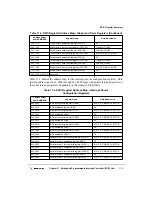
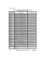
Table 11-2 defines the address map for the global EPIC and timer registers. See
Section 11.9, “Register Definitions,” for detailed register and field descriptions.
Table 11-2. EPIC Register Address Map—Global and Timer Registers
Address Offset
from EUMBBAR
Register Name
Field Mnemonics
0x4_1000
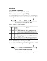
Feature reporting register (FRR)
NIRQ, NCPU, VID
0x4_1010
Reserved
—
0x4_1020
Global configuration register (GCR)
R (reset), M (mode)
0x4_1030
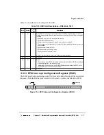
EPIC interrupt configuration register (EICR)
R (clock ratio), SIE
0x4_1040–0x4_1070
Reserved
—
0x4_1080
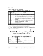
EPIC vendor identification register (EVI)
STEP, DEVICE_ID,
VENDOR_ID
0x4_1090
Processor initialization register (PI)
P0
0x4_10A0–0x4_10D0
Reserved
—
0x4_10E0
Spurious vector register (SVR)
VECTOR
0x4_10F0
Timer frequency reporting register (TFRR)
TIMER_FREQ
0x4_1100
Global timer 0 current count register (GTCCR0)
T (toggle), COUNT
0x4_1110
Global timer 0 base count register (GTBCR0)
CI, BASE_COUNT
0x4_1120
Global timer 0 vector/priority register (GTVPR0)
M, A, PRIORITY, VECTOR
0x4_1130
Global timer 0 destination register (GTDR0)
P0
0x4_1140
Global timer 1 current count register (GTCCR1)
T (toggle), COUNT
0x4_1150
Global timer 1 base count register (GTBCR1)
CI, BASE_COUNT
0x4_1160
Global timer 1 vector/priority register (GTVPR1)
M, A, PRIORITY, VECTOR
Summary of Contents for MPC8240
Page 1: ...MPC8240UM D Rev 1 1 2001 MPC8240 Integrated Processor User s Manual ...
Page 38: ...xviii MPC8240 Integrated Processor User s Manual TABLES Table Number Title Page Number ...
Page 48: ...xlviii MPC8240 Integrated Processor User s Manual Acronyms and Abbreviations ...
Page 312: ...6 94 MPC8240 Integrated Processor User s Manual ROM Flash Interface Operation ...
Page 348: ...7 36 MPC8240 Integrated Processor User s Manual PCI Host and Agent Modes ...
Page 372: ...8 24 MPC8240 Integrated Processor User s Manual DMA Register Descriptions ...
Page 394: ...9 22 MPC8240 Integrated Processor User s Manual I2O Interface ...
Page 412: ...10 18 MPC8240 Integrated Processor User s Manual Programming Guidelines ...
Page 454: ...12 14 MPC8240 Integrated Processor User s Manual Internal Arbitration ...
Page 466: ...13 12 MPC8240 Integrated Processor User s Manual Exception Latencies ...
Page 516: ...16 14 Watchpoint Trigger Applications ...
Page 538: ...B 16 MPC8240 Integrated Processor User s Manual Setting the Endian Mode of Operation ...
Page 546: ...C 8 MPC8240 Integrated Processor User s Manual ...
Page 640: ...INDEX Index 16 MPC8240 Integrated Processor User s Manual ...


