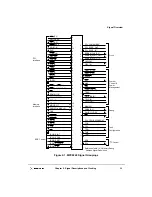

Chapter 2. Signal Descriptions and Clocking
2-17
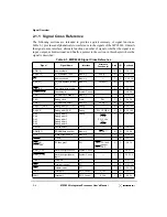
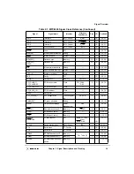
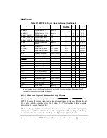
Detailed Signal Descriptions
2.2.2.2 Column Address Strobe (CAS[0:7])—Output
The eight column address strobe (CAS[0:7]) signals are outputs on the MPC8240. CAS0
connects to the most-significant byte select. CAS7 connects to the least-significant byte
select. When the MPC8240 is operating in 32-bit mode (see MCCR1[DBUS_SIZ[0:1]), the
CAS[0:3] signals are used. Following are the state meaning and timing comments for the
CASn output signals.
State Meaning
Asserted—Indicates that the DRAM (or EDO) column address is
valid and selects one of the columns in the row.
Negated—For DRAMs, it indicates CASn precharge, and that the
current DRAM data transfer has completed.
—or—
For EDO DRAMs, it indicates CASn precharge, and that the current
data transfer completes in the first clock cycle of CASn precharge.
Timing Comments
Assertion—The MPC8240 asserts CASn two to eight clock cycles
after the assertion of RASn (depending on the setting of the
MCCR3[RCD
2
] parameter). See Section 6.3.5, “FPM or EDO
DRAM Interface Timing,” for more information.
2.2.2.3 SDRAM Command Select (CS[0:7])—Output
The eight SDRAM command select (CS[0:7]) signals are output on the MPC8240.
Following are the state meaning and timing comments for the CSn output signals.
State Meaning
Asserted—Selects an SDRAM bank to perform a memory operation.
Negated—Indicates no SDRAM action during the current cycle.
Timing Comments
Assertion—The MPC8240 asserts the CSn signal to begin a memory
cycle. For SDRAM, CSn is valid on the rising edge of the
SDRAM_CLK[0:3] clock signals.
2.2.2.4 SDRAM Data Input/Output Mask (DQM[0:7])—Output
The eight SDRAM data input/output mask (DQM[0:7]) signals are outputs on the
MPC8240. Following are the state meaning and timing comments for the DQMn output
signals. DQM0 connects to the most significant byte select, and DQM7 connects to the least
significant byte select. Note that parity memory can be connected to any DQMn signal.
State Meaning
Asserted—Prevents writing to SDRAM. Note that the DQMn
signals are active-high for SDRAM. DQMn is part of the SDRAM
command encoding. See Section 6.2, “SDRAM Interface
Operation,” for more information.
Negated—Allows a read or write operation to SDRAM.
Timing Comments
Assertion—For SDRAM, DQMn is valid on the rising edge of the
SDRAM_CLK[0:3] clock signals during read or write cycles.
Summary of Contents for MPC8240
Page 1: ...MPC8240UM D Rev 1 1 2001 MPC8240 Integrated Processor User s Manual ...
Page 38: ...xviii MPC8240 Integrated Processor User s Manual TABLES Table Number Title Page Number ...
Page 48: ...xlviii MPC8240 Integrated Processor User s Manual Acronyms and Abbreviations ...
Page 312: ...6 94 MPC8240 Integrated Processor User s Manual ROM Flash Interface Operation ...
Page 348: ...7 36 MPC8240 Integrated Processor User s Manual PCI Host and Agent Modes ...
Page 372: ...8 24 MPC8240 Integrated Processor User s Manual DMA Register Descriptions ...
Page 394: ...9 22 MPC8240 Integrated Processor User s Manual I2O Interface ...
Page 412: ...10 18 MPC8240 Integrated Processor User s Manual Programming Guidelines ...
Page 454: ...12 14 MPC8240 Integrated Processor User s Manual Internal Arbitration ...
Page 466: ...13 12 MPC8240 Integrated Processor User s Manual Exception Latencies ...
Page 516: ...16 14 Watchpoint Trigger Applications ...
Page 538: ...B 16 MPC8240 Integrated Processor User s Manual Setting the Endian Mode of Operation ...
Page 546: ...C 8 MPC8240 Integrated Processor User s Manual ...
Page 640: ...INDEX Index 16 MPC8240 Integrated Processor User s Manual ...


