2-20
MPC8240 Integrated Processor User’s Manual
Detailed Signal Descriptions
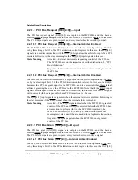
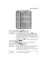
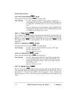
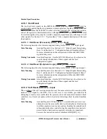
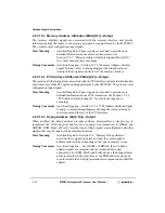
2.2.2.9.1 Memory Data Bus (MDH[0:31], MDL[0:31])—Output
Following are the state meaning and timing comments for the memory data bus as output
signals.
State Meaning
Asserted/Negated—Represents the value of data being driven by the
MPC8240.
Timing Comments
Assertion/Negation—For DRAM accesses, the data bus signals are
valid when CAS[0:7] and WE are asserted. For SDRAM, the data
bus signals are valid on the next rising edge of SDRAM_CLK[0:3]
after DQM[0:7] is asserted for a write command. For ROM/Flash
memory and Port X, the data bus signals are valid on the assertion of
RCS0.
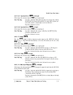
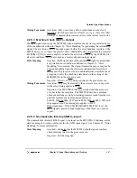
2.2.2.9.2 Memory Data Bus (MDH[0:31], MDL[0:31])—Input
Following are the state meaning and timing comments for the data bus as input signals.
Note that MDL0 is a reset configuration input signal.
State Meaning
Asserted/Negated—Represents the value of data being driven by the
memory subsystem on a read.
Timing Comments
Assertion/Negation—For a memory read transaction, the data bus
signals are valid at a time dependent on the memory interface
configuration parameters. Refer to Chapter 4, “Configuration
Registers,” and Chapter 6, “MPC8240 Memory Interface,” for more
information.
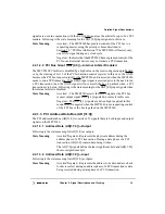
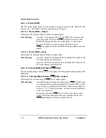
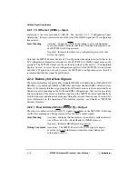
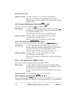
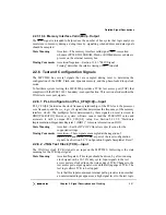
2.2.2.10 Data Parity/ECC (PAR[0:7])
The eight data parity/ECC (PAR[0:7]) signals are both input and output signals on the
MPC8240.
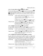
2.2.2.10.1 Data Parity (PAR[0:7])—Output
Following are the state meaning and timing comments for PAR[0:7] as output signals.
State Meaning
Asserted/Negated—Represents the byte parity or ECC bits being
written to memory (PAR0 is the most-significant parity bit and
corresponds to byte lane 0 which is selected by CAS0 or DQM0).
The data parity signals are asserted or negated as appropriate to
provide odd parity (including the parity bit) or ECC.
Timing Comments
Assertion/Negation—PAR[0:7] are valid concurrent with
MDH[0:31] and MDL[0:31].
Summary of Contents for MPC8240
Page 1: ...MPC8240UM D Rev 1 1 2001 MPC8240 Integrated Processor User s Manual ...
Page 38: ...xviii MPC8240 Integrated Processor User s Manual TABLES Table Number Title Page Number ...
Page 48: ...xlviii MPC8240 Integrated Processor User s Manual Acronyms and Abbreviations ...
Page 312: ...6 94 MPC8240 Integrated Processor User s Manual ROM Flash Interface Operation ...
Page 348: ...7 36 MPC8240 Integrated Processor User s Manual PCI Host and Agent Modes ...
Page 372: ...8 24 MPC8240 Integrated Processor User s Manual DMA Register Descriptions ...
Page 394: ...9 22 MPC8240 Integrated Processor User s Manual I2O Interface ...
Page 412: ...10 18 MPC8240 Integrated Processor User s Manual Programming Guidelines ...
Page 454: ...12 14 MPC8240 Integrated Processor User s Manual Internal Arbitration ...
Page 466: ...13 12 MPC8240 Integrated Processor User s Manual Exception Latencies ...
Page 516: ...16 14 Watchpoint Trigger Applications ...
Page 538: ...B 16 MPC8240 Integrated Processor User s Manual Setting the Endian Mode of Operation ...
Page 546: ...C 8 MPC8240 Integrated Processor User s Manual ...
Page 640: ...INDEX Index 16 MPC8240 Integrated Processor User s Manual ...

