
10-36
MPC8260 PowerQUICC II UserÕs Manual
MOTOROLA
Part III. The Hardware Interface
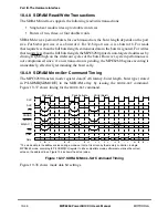
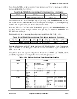
10.4.4 Page-Mode Support and Pipeline Accesses
The SDRAM interface supports back-to-back page mode. A page remains open as long as
back-to-back accesses that hit the page are generated on the bus. The page is closed once
the bus becomes idle unless OR
x
[PMSEL] is set.
The use of SDRAM pipelining allows data phases to occur on with zero bubbles for CPM
accesses and with one bubble for core accesses, as required by the 60x bus speciÞcation.
If ETM/LETM = 1, the use of SDRAM pipelining also allows for back-to-back data
phases to occur with zero clocks of separation for CPM accesses and with one clock of
separation for core accesses, as required by the 60x bus speciÞcation.
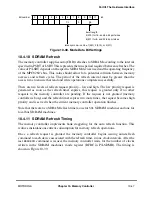
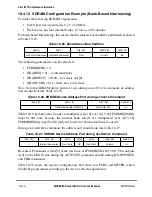
10.4.5 Bank Interleaving
The SDRAM interface supports bank interleaving. This means that if a missed page is in a
different SDRAM bank than the currently open page, the SDRAM machine Þrst issues an
ACTIVATE
command to the new page and later issues a
DEACTIVATE
command to the old
page, thus eliminating the
DEACTIVATE
time overhead.
This procedure can be done if both pages reside on different SDRAM devices or on
different internal SDRAM banks. The second option can be disabled by setting OR
x
[IBID].
The user should set this bit if the BNKSEL pins are not used in 60x-compatible mode.
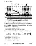
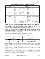
PRECHARGE
(
SINGLE
BANK
/
ALL
BANKS
)
Restores data from the sense ampliÞers to the appropriate row. Also initializes the sense ampliÞers to
prepare for reading another row in the SDRAM array. A
PRECHARGE
command must be issued after a
read or write if the row address changes on the next access. Note that the MPC8260 uses the SDA10
pin to distinguish the
PRECHARGE
-
ALL
-
BANKS
command. The SDRAMs must be compatible with this
format.
READ
Latches the column address and transfers data from the selected sense ampliÞer to the output buffer
as determined by the column address. During each successive clock, additional data is output without
additional
READ
commands. The amount of data transferred is determined by the burst size. At the end
of the burst, the page remains open.
REFRESH
Causes a row to be read in both memory banks (JEDEC SDRAM) as determined by the refresh row
address counter (similar to CBR). The refresh row address counter is internal to the SDRAM device.
After being read, a row is automatically rewritten into the memory array. Both banks must be in a
precharged state before executing
REFRESH
.
WRITE
Latches the column address and transfers data from the data signals to the selected sense ampliÞer
as determined by the column address. During each successive clock, additional data is transferred to
the sense ampliÞers from the data signals without additional
WRITE
commands. The amount of data
transferred is determined by the burst size. At the end of the burst, the page remains open.
Table 10-18. SDRAM Interface Commands (Continued)
Command
Description
Summary of Contents for MPC8260 PowerQUICC II
Page 1: ...MPC8260UM D 4 1999 Rev 0 MPC8260 PowerQUICC II UserÕs Manual ª ª ...
Page 66: ...lxvi MPC8260 PowerQUICC II UserÕs Manual MOTOROLA ...
Page 88: ...1 18 MPC8260 PowerQUICC II UserÕs Manual MOTOROLA Part I Overview ...
Page 120: ...2 32 MPC8260 PowerQUICC II UserÕs Manual MOTOROLA Part I Overview ...
Page 138: ...Part II iv MPC8260 PowerQUICC II UserÕs Manual MOTOROLA Part II Configuration and Reset ...
Page 184: ...4 46 MPC8260 PowerQUICC II UserÕs Manual MOTOROLA Part II ConÞguration and Reset ...
Page 202: ...Part III vi MPC8260 PowerQUICC II UserÕs Manual MOTOROLA Part III The Hardware Interface ...
Page 266: ...8 34 MPC8260 PowerQUICC II UserÕs Manual MOTOROLA Part III The Hardware Interface ...
Page 382: ...10 106 MPC8260 PowerQUICC II UserÕs Manual MOTOROLA Part III The Hardware Interface ...
Page 392: ...11 10 MPC8260 PowerQUICC II UserÕs Manual MOTOROLA Part III The Hardware Interface ...
Page 430: ...Part IV viii MOTOROLA Part IV Communications Processor Module ...
Page 490: ...14 36 MPC8260 PowerQUICC II UserÕs Manual MOTOROLA Part IV Communications Processor Module ...
Page 524: ...17 10 MPC8260 PowerQUICC II UserÕs Manual MOTOROLA Part IV Communications Processor Module ...
Page 556: ...18 32 MPC8260 PowerQUICC II UserÕs Manual MOTOROLA Part IV Communications Processor Module ...
Page 584: ...19 28 MPC8260 PowerQUICC II UserÕs Manual MOTOROLA Part IV Communications Processor Module ...
Page 632: ...21 24 MPC8260 PowerQUICC II UserÕs Manual MOTOROLA Part IV Communications Processor Module ...
Page 652: ...22 20 MPC8260 PowerQUICC II UserÕs Manual MOTOROLA Part IV Communications Processor Module ...
Page 668: ...23 16 MPC8260 PowerQUICC II UserÕs Manual MOTOROLA Part IV Communications Processor Module ...
Page 758: ...27 28 MPC8260 PowerQUICC II UserÕs Manual MOTOROLA Part IV Communications Processor Module ...
Page 780: ...28 22 MPC8260 PowerQUICC II UserÕs Manual MOTOROLA Part IV Communications Processor Module ...
Page 874: ...29 94 MPC8260 PowerQUICC II UserÕs Manual MOTOROLA Part IV Communications Processor Module ...
Page 920: ...31 18 MPC8260 PowerQUICC II UserÕs Manual MOTOROLA Part IV Communications Processor Module ...
Page 980: ...A 4 MPC8260 PowerQUICC II UserÕs Manual MOTOROLA Appendixes ...
Page 1002: ...Index 22 MPC8260 PowerQUICC II UserÕs Manual MOTOROLA INDEX ...
Page 1006: ......