10-102
MPC8260 PowerQUICC II UserÕs Manual
MOTOROLA
Part III. The Hardware Interface
¥
PSDVAL as a termination to a partial transaction (such as port-size beat access).
¥
Internal SDRAM bank selects (BNKSEL[0Ð2]) to allow SDRAM bank interleaving,
as described in Section 10.9.4, ÒUsing BNKSEL SIgnals in Single-MPC8260 Bus
Mode.Ó
10.9.4 Using BNKSEL SIgnals in Single-MPC8260 Bus Mode
The BNKSEL signals provide the following functionality in single-MPC8260 bus mode
¥
If bank-based interleaving is used, BNKSEL signals facilitate compatibility with
SDRAMs that have different numbers of row or column address lines. The address
lines of the MPC8260 bus and the BNKSEL lines can be routed independently to the
address lines and BA lines of the DIMM. Note that all SDRAMs populated on an
MPC8260 bus must still have the same organization. This ßexibility merely allows
the SDRAMs to be populated as a group with larger or smaller devices as
appropriate.
If BNKSEL lines were not used, the number of row and column address lines of the
SDRAMs would affect which MPC8260 address bus lines on which the bank select
signals would be driven, and would thus require that the BA signals of the SDRAMs
be routed to those address lines, thus limiting ßexibility.
¥
If BCR[HP] is programmed, BNKSEL signals facilitate logic analysis of the system.
Otherwise, the logic analyzer equipment must understand the address multiplexing
scheme of the board and intelligently reconstruct the address of bus transactions.
10.9.5 Address Incrementing for External Bursting Masters
BADDR[27Ð31] should be used to generate addresses to memory devices for burst
accesses. In 60x-compatible mode, when a master initiates an external bus transaction, it
reßects the value of A[27Ð31] on the Þrst clock cycle of the memory access. These signals
are latched by the memory controller and on subsequent clock cycles, BADDR[27Ð31]
increments as programmed in the UPM or after each data beat is sampled in the GPCM or
after each
READ
/
WRITE
command in the SDRAM machine (the SDRAM machine uses
BADDR only for port sizes of 16 or 8 bits).
10.9.6 External Masters Timing
External and internal masters have similar memory access timings. However, because it
takes more time to decode the addresses of external masters, memory accesses by external
masters start one cycle later than those of internal masters.
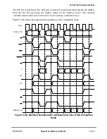
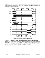
As soon as the external master asserts TS, the memory controller compares the address with
each of its deÞned valid banks. If a match is found, the memory controller asserts the
address latch enable (ALE) and control signals to the memory devices. The memory
controller asserts PSDVAL for each data beat to indicate data beat termination on write
transactions and data valid on read transactions.
Summary of Contents for MPC8260 PowerQUICC II
Page 1: ...MPC8260UM D 4 1999 Rev 0 MPC8260 PowerQUICC II UserÕs Manual ª ª ...
Page 66: ...lxvi MPC8260 PowerQUICC II UserÕs Manual MOTOROLA ...
Page 88: ...1 18 MPC8260 PowerQUICC II UserÕs Manual MOTOROLA Part I Overview ...
Page 120: ...2 32 MPC8260 PowerQUICC II UserÕs Manual MOTOROLA Part I Overview ...
Page 138: ...Part II iv MPC8260 PowerQUICC II UserÕs Manual MOTOROLA Part II Configuration and Reset ...
Page 184: ...4 46 MPC8260 PowerQUICC II UserÕs Manual MOTOROLA Part II ConÞguration and Reset ...
Page 202: ...Part III vi MPC8260 PowerQUICC II UserÕs Manual MOTOROLA Part III The Hardware Interface ...
Page 266: ...8 34 MPC8260 PowerQUICC II UserÕs Manual MOTOROLA Part III The Hardware Interface ...
Page 382: ...10 106 MPC8260 PowerQUICC II UserÕs Manual MOTOROLA Part III The Hardware Interface ...
Page 392: ...11 10 MPC8260 PowerQUICC II UserÕs Manual MOTOROLA Part III The Hardware Interface ...
Page 430: ...Part IV viii MOTOROLA Part IV Communications Processor Module ...
Page 490: ...14 36 MPC8260 PowerQUICC II UserÕs Manual MOTOROLA Part IV Communications Processor Module ...
Page 524: ...17 10 MPC8260 PowerQUICC II UserÕs Manual MOTOROLA Part IV Communications Processor Module ...
Page 556: ...18 32 MPC8260 PowerQUICC II UserÕs Manual MOTOROLA Part IV Communications Processor Module ...
Page 584: ...19 28 MPC8260 PowerQUICC II UserÕs Manual MOTOROLA Part IV Communications Processor Module ...
Page 632: ...21 24 MPC8260 PowerQUICC II UserÕs Manual MOTOROLA Part IV Communications Processor Module ...
Page 652: ...22 20 MPC8260 PowerQUICC II UserÕs Manual MOTOROLA Part IV Communications Processor Module ...
Page 668: ...23 16 MPC8260 PowerQUICC II UserÕs Manual MOTOROLA Part IV Communications Processor Module ...
Page 758: ...27 28 MPC8260 PowerQUICC II UserÕs Manual MOTOROLA Part IV Communications Processor Module ...
Page 780: ...28 22 MPC8260 PowerQUICC II UserÕs Manual MOTOROLA Part IV Communications Processor Module ...
Page 874: ...29 94 MPC8260 PowerQUICC II UserÕs Manual MOTOROLA Part IV Communications Processor Module ...
Page 920: ...31 18 MPC8260 PowerQUICC II UserÕs Manual MOTOROLA Part IV Communications Processor Module ...
Page 980: ...A 4 MPC8260 PowerQUICC II UserÕs Manual MOTOROLA Appendixes ...
Page 1002: ...Index 22 MPC8260 PowerQUICC II UserÕs Manual MOTOROLA INDEX ...
Page 1006: ......


