background image

29-16

MPC8260 PowerQUICC II UserÕs Manual

MOTOROLA

Part IV.  Communications Processor Module

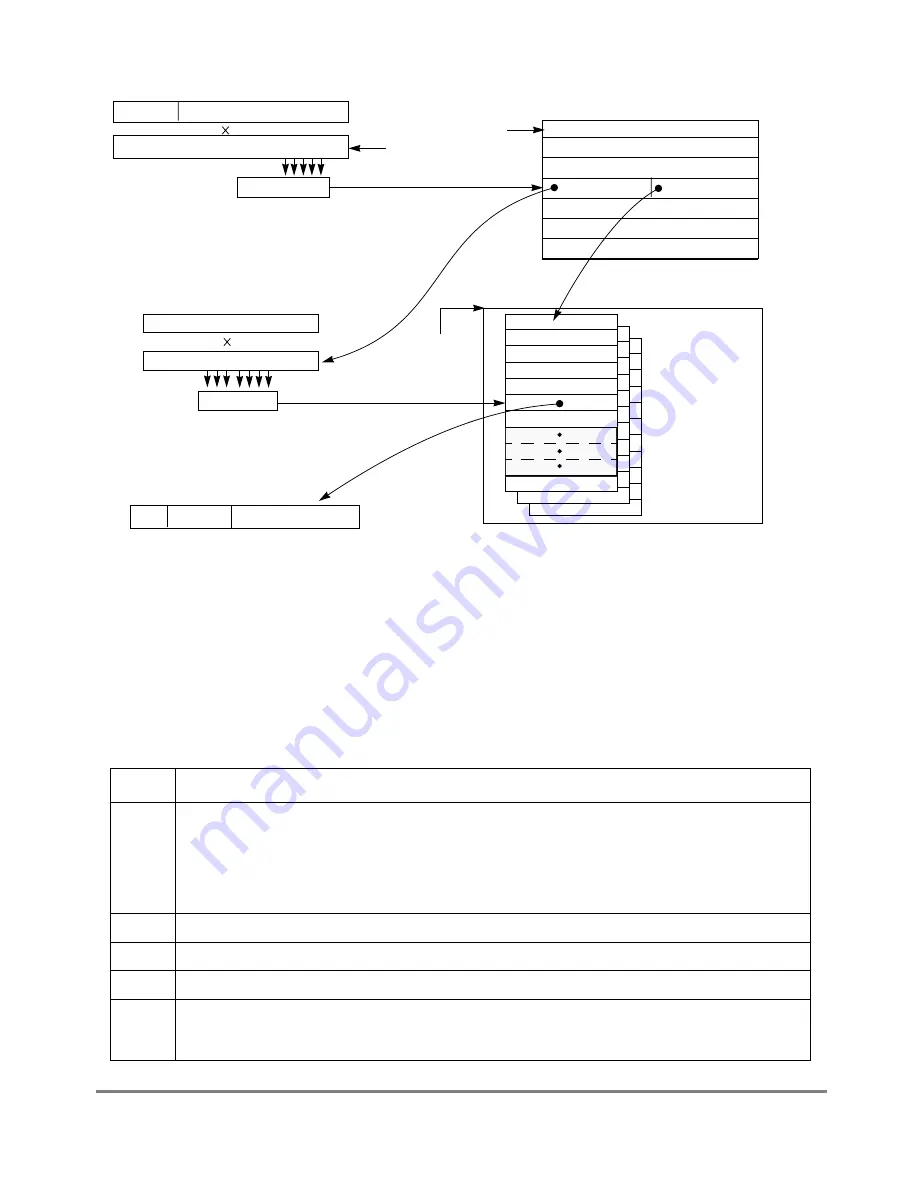
Figure 29-5. Address Compression Mechanism

Figure 29-5 shows VP_MASK selecting Þve VPI bits to index the VP-level table. The VP-
level table entry contains the 16-bit mask (VC_MASK) and the VC-level table offset
(VCOFFSET) for the next level of address mapping. The VC_MASK selects VCI bits 4Ð
10, which is used with VCT_BASE and VCOFFSET to indicate the received cellÕs channel
code. 

Table 29-3. Field Descriptions for Address Compression  

Field Description 

PHY 
Addr 

In multiple PHY mode, this Þeld contains the 4 least-signiÞcant bits of the current channelÕs physical 
address. Because this comparison Þeld is limited to 4 bits, two sets of look-up tables are needed if using 
more than 16 PHYs.The msb of the PHY address lines (bit 4) selects between the two sets of tables. If the 
msb is zero, the CP accesses the tables at VPT_BASE and VCT_BASE; if the msb is set, the CP uses 
VPT1_BASE and VCT1_BASE. See Section 15.4.1, ÒCMX UTOPIA Address Register (CMXUAR).Ó
In single PHY mode, clear this Þeld.

VCI, VPI

The VCI and VPI of the current channel.

Ch Code Pointer to internal or external connection table.

Ñ

Reserved, should be cleared.

MS

Match status.
0 Match was found.
1 Match was not found.

32-bit entries

VP-level addressing table

 VPI

0000  


00011111 

VPpointer

VPT_BASE

VCOFFSET

VC_MASK

VCI

00000111 11110000

VCpointer

32-bit entries

VC-level addressing tables 

VCT_BASE

VP_MASK

16 bit

16 bit

PHY Addr

0000 

16 bit

12 bit

4 bit

(in external memory)

(in dual-port RAM recommended)

Ch Code[15Ð0]

Ñ

16 bit

15 bit 

MS

1 bit

31

0

31

0

0b00011

Summary of Contents for MPC8260 PowerQUICC II

Page 1: ...MPC8260UM D 4 1999 Rev 0 MPC8260 PowerQUICC II UserÕs Manual ª ª ...

Page 2: ...pplications intended to support or sustain life or for any other application in which the failure of the Motorola product could create a situation where personal injury or death may occur Should Buyer purchase or use Motorola products for any such unintended or unauthorized application Buyer shall indemnify and hold Motorola and its officers employees subsidiaries affiliates and distributors harml...

Page 3: ...and IDMA Emulation Serial Communications Controllers SCCs SCC UART Mode SCC HDLC Mode SCC BISYNC Mode SCC Transparent Mode SCC Ethernet Mode SCC AppleTalk Mode Serial Management Controllers SMCs Multi Channel Controllers MCCs Fast Communications Controllers ATM Controller Fast Ethernet Controller FCC HDLC Controller FCC Transparent Controller Serial Peripheral Interface SPI I2C Controller Parallel...

Page 4: ...and IDMA Emulation Serial Communications Controllers SCCs SCC UART Mode SCC HDLC Mode SCC BISYNC Mode SCC Transparent Mode SCC Ethernet Mode SCC AppleTalk Mode Serial Management Controllers SMCs Multi Channel Controllers MCCs Fast Communications Controllers ATM Controller Fast Ethernet Controller FCC HDLC Controller FCC Transparent Controller Serial Peripheral Interface SPI I2C Controller Parallel...

Page 5: ...2 2 System Interface Unit SIU 1 6 1 2 3 Communications Processor Module CPM 1 6 1 3 Software Compatibility Issues 1 7 1 3 1 Signals 1 7 1 4 Differences between MPC860 and MPC8260 1 9 1 5 Serial Protocol Table 1 9 1 6 MPC8260 Configurations 1 10 1 6 1 Pin Configurations 1 10 1 6 2 Serial Performance 1 10 1 7 MPC8260 Application Examples 1 11 1 7 1 Examples of Communication Systems 1 11 1 7 1 1 Remo...

Page 6: ... 2 2 6 2 Cache Units 2 8 2 3 Programming Model 2 8 2 3 1 Register Set 2 8 2 3 1 1 PowerPC Register Set 2 9 2 3 1 2 MPC8260 Specific Registers 2 11 2 3 1 2 1 Hardware Implementation Dependent Register 0 HID0 2 11 2 3 1 2 2 Hardware Implementation Dependent Register 1 HID1 2 14 2 3 1 2 3 Hardware Implementation Dependent Register 2 HID2 2 15 2 3 1 2 4 Processor Version Register PVR 2 16 2 3 2 PowerP...

Page 7: ...rrupt Configuration 4 8 4 2 2 Interrupt Source Priorities 4 9 4 2 2 1 SCC FCC and MCC Relative Priority 4 12 4 2 2 2 PIT TMCNT and IRQ Relative Priority 4 12 4 2 2 3 Highest Priority Interrupt 4 13 4 2 3 Masking Interrupt Sources 4 13 4 2 4 Interrupt Vector Generation and Calculation 4 14 4 2 4 1 Port C External Interrupts 4 16 4 3 Programming Model 4 17 4 3 1 Interrupt Controller Registers 4 17 4...

Page 8: ...ansfer Error Status and Control Register 2 L_TESCR2 4 39 4 3 2 14 Time Counter Status and Control Register TMCNTSC 4 40 4 3 2 15 Time Counter Register TMCNT 4 41 4 3 2 16 Time Counter Alarm Register TMCNTAL 4 41 4 3 3 Periodic Interrupt Registers 4 42 4 3 3 1 Periodic Interrupt Status and Control Register PISCR 4 42 4 3 3 2 Periodic Interrupt Timer Count Register PITC 4 43 4 3 3 3 Periodic Interru...

Page 9: ...6 7 2 2 1 Transfer Start TS 7 6 7 2 2 1 1 Transfer Start TS ÑOutput 7 6 7 2 2 2 Transfer Start TS ÑInput 7 6 7 2 3 Address Transfer Signals 7 7 7 2 3 1 Address Bus A 0Ð31 7 7 7 2 3 1 1 Address Bus A 0Ð31 ÑOutput 7 7 7 2 3 1 2 Address Bus A 0Ð31 ÑInput 7 7 7 2 4 Address Transfer Attribute Signals 7 7 7 2 4 1 Transfer Type TT 0Ð4 7 8 7 2 4 1 1 Transfer Type TT 0Ð4 ÑOutput 7 8 7 2 4 1 2 Transfer Type...

Page 10: ...2 2 Data Bus Parity DP 0Ð7 ÑInput 7 15 7 2 8 Data Transfer Termination Signals 7 15 7 2 8 1 Transfer Acknowledge TA 7 15 7 2 8 1 1 Transfer Acknowledge TA ÑInput 7 15 7 2 8 1 2 Transfer Acknowledge TA ÑOutput 7 16 7 2 8 2 Transfer Error Acknowledge TEA 7 16 7 2 8 2 1 Transfer Error Acknowledge TEA ÑInput 7 16 7 2 8 2 2 Transfer Error Acknowledge TEA ÑOutput 7 17 7 2 8 3 Partial Data Valid Indicati...

Page 11: ... 8 5 Data Tenure Operations 8 26 8 5 1 Data Bus Arbitration 8 26 8 5 2 Data Streaming Mode 8 27 8 5 3 Data Bus Transfers and Normal Termination 8 27 8 5 4 Effect of ARTRY Assertion on Data Transfer and Arbitration 8 28 8 5 5 Port Size Data Bus Transfers and PSDVAL Termination 8 28 8 5 6 Data Bus Termination by Assertion of TEA 8 30 8 6 Memory CoherencyÑMEI Protocol 8 31 8 7 Processor State Signals...

Page 12: ... 11 10 2 13 Partial Data Valid Indication PSDVAL 10 12 10 3 Register Descriptions 10 13 10 3 1 Base Registers BRx 10 14 10 3 2 Option Registers ORx 10 16 10 3 3 60x SDRAM Mode Register PSDMR 10 21 10 3 4 Local Bus SDRAM Mode Register LSDMR 10 24 10 3 5 Machine A B C Mode Registers MxMR 10 26 10 3 6 Memory Data Register MDR 10 28 10 3 7 Memory Address Register MAR 10 29 10 3 8 60x Bus Assigned UPM ...

Page 13: ...age Based Interleaving 10 48 10 4 13 SDRAM Configuration Example Bank Based Interleaving 10 50 10 5 General Purpose Chip Select Machine GPCM 10 51 10 5 1 Timing Configuration 10 52 10 5 1 1 Chip Select Assertion Timing 10 53 10 5 1 2 Chip Select and Write Enable Deassertion Timing 10 54 10 5 1 3 Relaxed Timing 10 55 10 5 1 4 Output Enable OE Timing 10 57 10 5 1 5 Programmable Wait State Configurat...

Page 14: ... Example 10 100 10 9 External Master Support 60x Compatible Mode 10 101 10 9 1 60x Compatible External Masters 10 101 10 9 2 MPC8260 Type External Masters 10 101 10 9 3 Extended Controls in 60x Compatible Mode 10 101 10 9 4 Using BNKSEL SIgnals in Single MPC8260 Bus Mode 10 102 10 9 5 Address Incrementing for External Bursting Masters 10 102 10 9 6 External Masters Timing 10 102 10 9 6 1 Example o...

Page 15: ...3 9 RISC Microcode Revision Number 13 10 13 4 Command Set 13 11 13 4 1 CP Command Register CPCR 13 11 13 4 1 1 CP Commands 13 13 13 4 2 Command Register Example 13 15 13 4 3 Command Execution Latency 13 15 13 5 Dual Port RAM 13 15 13 5 1 Buffer Descriptors BDs 13 17 13 5 2 Parameter RAM 13 17 13 6 RISC Timer Tables 13 18 13 6 1 RISC Timer Table Parameter RAM 13 19 13 6 2 RISC Timer Command Registe...

Page 16: ...4 5 4 SI Command Register SIxCMDR 14 24 14 5 5 SI Status Registers SIxSTR 14 25 14 6 Serial Interface IDL Interface Support 14 25 14 6 1 IDL Interface Example 14 26 14 6 2 IDL Interface Programming 14 29 14 7 Serial Interface GCI Support 14 31 14 7 1 SI GCI Activation Deactivation Procedure 14 33 14 7 2 Serial Interface GCI Programming 14 33 14 7 2 1 Normal Mode GCI Programming 14 33 14 7 2 2 SCIT...

Page 17: ...apter 18 SDMA Channels and IDMA Emulation 18 1 SDMA Bus Arbitration and Bus Transfers 18 2 18 2 SDMA Registers 18 3 18 2 1 SDMA Status Register SDSR 18 3 18 2 2 SDMA Mask Register SDMR 18 4 18 2 3 SDMA Transfer Error Address Registers PDTEA and LDTEA 18 4 18 2 4 SDMA Transfer Error MSNUM Registers PDTEM and LDTEM 18 4 18 3 IDMA Emulation 18 5 18 4 IDMA Features 18 5 18 5 IDMA Transfers 18 6 18 5 1...

Page 18: ... 9 2 stop_idma Command 18 26 18 10 IDMA Bus Exceptions 18 27 18 10 1 Externally Recognizing IDMA Operand Transfers 18 27 18 11 Programming the Parallel I O Registers 18 28 18 12 IDMA Programming Examples 18 29 18 12 1 Peripheral to Memory Mode 60x Bus to Local Bus ÑIDMA2 18 29 18 12 2 Memory to Peripheral Fly By Mode Both on 60x Bus ÑIDMA3 18 30 Chapter 19 Serial Communications Controllers SCCs 19...

Page 19: ...Mode 20 3 20 4 SCC UART Parameter RAM 20 4 20 5 Data Handling Methods Character or Message Based 20 5 20 6 Error and Status Reporting 20 6 20 7 SCC UART Commands 20 6 20 8 Multidrop Systems and Address Recognition 20 7 20 9 Receiving Control Characters 20 8 20 10 Hunt Mode Receiver 20 10 20 11 Inserting Control Characters into the Transmit Data Stream 20 10 20 12 Sending a Break Transmitter 20 11 ...

Page 20: ...1 13 2 SCC HDLC Programming Example 2 21 16 21 14 HDLC Bus Mode with Collision Detection 21 17 21 14 1 HDLC Bus Features 21 19 21 14 2 Accessing the HDLC Bus 21 19 21 14 3 Increasing Performance 21 20 21 14 4 Delayed RTS Mode 21 21 21 14 5 Using the Time Slot Assigner TSA 21 22 21 14 6 HDLC Bus Protocol Programming 21 23 21 14 6 1 Programming GSMR and PSMR for the HDLC Bus Protocol 21 23 21 14 6 2...

Page 21: ...3 4 1 3 Transparent Mode without Explicit Synchronization 23 5 23 4 2 Synchronization and the TSA 23 5 23 4 2 1 Inline Synchronization Pattern 23 6 23 4 2 2 Inherent Synchronization 23 6 23 4 3 End of Frame Detection 23 6 23 5 CRC Calculation in Transparent Mode 23 6 23 6 SCC Transparent Parameter RAM 23 6 23 7 SCC Transparent Commands 23 7 23 8 Handling Errors in the Transparent Controller 23 8 2...

Page 22: ...24 20 SCC Ethernet Event Register SCCE Mask Register SCCM 24 21 24 21 SCC Ethernet Programming Example 24 23 Chapter 25 SCC AppleTalk Mode 25 1 Operating the LocalTalk Bus 25 1 25 2 Features 25 2 25 3 Connecting to AppleTalk 25 3 25 4 Programming the SCC in AppleTalk Mode 25 3 25 4 1 Programming the GSMR 25 3 25 4 2 Programming the PSMR 25 4 25 4 3 Programming the TODR 25 4 25 4 4 SCC AppleTalk Pr...

Page 23: ...SMC Transparent Channel Reception Process 26 22 26 4 4 Using SMSYN for Synchronization 26 22 26 4 5 Using the Time Slot Assigner TSA for Synchronization 26 23 26 4 6 SMC Transparent Commands 26 25 26 4 7 Handling Errors in the SMC Transparent Controller 26 25 26 4 8 SMC Transparent RxBD 26 26 26 4 9 SMC Transparent TxBD 26 27 26 4 10 SMC Transparent Event Register SMCE Mask Register SMCM 26 28 26 ...

Page 24: ...ions 27 17 27 10 1 MCC Event Register MCCE Mask Register MCCM 27 18 27 10 1 1 Interrupt Table Entry 27 19 27 11 MCC Buffer Descriptors 27 21 27 11 1 Receive Buffer Descriptor RxBD 27 21 27 11 2 Transmit Buffer Descriptor TxBD 27 23 27 12 MCC Initialization and Start Stop Sequence 27 24 27 12 1 Single Channel Initialization 27 25 27 12 2 Super Channel Initialization 27 26 27 13 MCC Latency and Perf...

Page 25: ...odes 29 6 29 2 2 Receiver Overview 29 6 29 2 2 1 AAL5 Receiver Overview 29 7 29 2 2 2 AAL1 Receiver Overview 29 7 29 2 2 3 AAL0 Receiver Overview 29 8 29 2 3 Performance Monitoring 29 8 29 2 4 ABR Flow Control 29 8 29 3 ATM Pace Control APC Unit 29 8 29 3 1 APC Modes and ATM Service Types 29 8 29 3 2 APC Unit Scheduling Mechanism 29 9 29 3 3 Determining the Scheduling Table Size 29 10 29 3 3 1 Det...

Page 26: ...r OAM Definitions 29 27 29 6 2 Virtual Path F4 Flow Mechanism 29 28 29 6 3 Virtual Channel F5 Flow Mechanism 29 28 29 6 4 Receiving OAM F4 or F5 Cells 29 28 29 6 5 Transmitting OAM F4 or F5 Cells 29 29 29 6 6 Performance Monitoring 29 29 29 6 6 1 Running a Performance Block Test 29 30 29 6 6 2 PM Block Monitoring 29 30 29 6 6 3 PM Block Generation 29 31 29 6 6 4 BRC Performance Calculations 29 32 ...

Page 27: ...61 29 10 4 1 APC Parameter Tables 29 62 29 10 4 2 APC Priority Table 29 63 29 10 4 3 APC Scheduling Tables 29 63 29 10 5 ATM Controller Buffer Descriptors BDs 29 64 29 10 5 1 Transmit Buffer Operations 29 64 29 10 5 2 Receive Buffers Operation 29 65 29 10 5 2 1 Static Buffer Allocation 29 65 29 10 5 2 2 Global Buffer Allocation 29 66 29 10 5 2 3 Free Buffer Pools 29 67 29 10 5 2 4 Free Buffer Pool...

Page 28: ... Controller for Maximum CPM Performance 29 92 29 16 1 Using Transmit Internal Rate Mode 29 92 29 16 2 APC Configuration 29 93 29 16 3 Buffer Configuration 29 93 Chapter 30 Fast Ethernet Controller 30 1 Fast Ethernet on the MPC8260 30 2 30 2 Features 30 3 30 3 Connecting the MPC8260 to Fast Ethernet 30 4 30 4 Ethernet Channel Frame Transmission 30 5 30 5 Ethernet Channel Frame Reception 30 7 30 6 F...

Page 29: ... 31 10 FCC Status Register FCCS 31 16 Chapter 32 FCC Transparent Controller 32 1 Features 32 2 32 2 Transparent Channel Operation 32 2 32 3 Achieving Synchronization in Transparent Mode 32 2 32 3 1 In Line Synchronization Pattern 32 3 32 3 2 External Synchronization Signals 32 3 32 3 3 Transparent Synchronization Example 32 4 Chapter 33 Serial Peripheral Interface SPI 33 1 Features 33 2 33 2 SPI C...

Page 30: ...C Controller Transfers 34 3 34 3 1 I2 C Master Write Slave Read 34 4 34 3 2 I2 C Loopback Testing 34 4 34 3 3 I2C Master Read Slave Write 34 4 34 3 4 I2 C Multi Master Considerations 34 5 34 4 I2 C Registers 34 6 34 4 1 I2 C Mode Register I2MOD 34 6 34 4 2 I2 C Address Register I2ADD 34 7 34 4 3 I2C Baud Rate Generator Register I2BRG 34 7 34 4 4 I2 C Event Mask Registers I2CER I2CMR 34 8 34 4 5 I2...

Page 31: ...tions Registers AÐD PSORAÐPSORD 35 4 35 3 Port Block Diagram 35 6 35 4 Port Pins Functions 35 6 35 4 1 General Purpose I O Pins 35 7 35 4 2 Dedicated Pins 35 7 35 5 Ports Tables 35 7 35 6 Interrupts from Port C 35 19 Appendix A Register Quick Reference Guide A 1 PowerPC RegistersÑUser Registers A 1 A 2 PowerPC RegistersÑSupervisor Registers A 2 A 3 MPC8260 Specific SPRs A 3 Glossary Index ...

Page 32: ...xxxii MPC8260 PowerQUICC II UserÕs Manual MOTOROLA CONTENTS Paragraph Number Title Page Number ...

Page 33: ...ation Register 0 HID0 2 11 2 4 Hardware Implementation Register 1 HID1 2 15 2 5 Hardware Implementation Dependent Register 2 HID2 2 15 2 6 Data Cache Organization 2 20 4 1 SIU Block Diagram 4 1 4 2 System Configuration and Protection Logic 4 3 4 3 Timers Clock Generation 4 4 4 4 TMCNT Block Diagram 4 5 4 5 PIT Block Diagram 4 5 4 6 Software Watchdog Timer Service State Diagram 4 6 4 7 Software Wat...

Page 34: ...rm Register TMCNTAL 4 42 4 38 Periodic Interrupt Status and Control Register PISCR 4 42 4 39 Periodic interrupt Timer Count Register PITC 4 43 4 40 Periodic Interrupt Timer Register PITR 4 44 5 1 Reset Status Register RSR 5 4 5 2 Reset Mode Register RMR 5 5 5 3 Hard Reset Configuration Word 5 8 5 4 Single Chip with Default Configuration 5 10 5 5 Configuring a Single Chip from EPROM 5 10 5 6 Config...

Page 35: ...T 10 31 10 17 Local Bus Assigned SDRAM Refresh Timer LSRT 10 32 10 18 Memory Refresh Timer Prescaler Register MPTPR 10 32 10 19 128 Mbyte SDRAM Eight Bank Configuration Banks 1 and 8 Shown 10 34 10 20 PRETOACT 2 2 Clock Cycles 10 39 10 21 ACTTORW 2 2 Clock Cycles 10 39 10 22 CL 2 2 Clock Cycles 10 40 10 23 LDOTOPRE 2 2 Clock Cycles 10 40 10 24 WRC 2 2 Clock Cycles 10 41 10 25 RFRC 4 6 Clock Cycles...

Page 36: ...6 10 58 Memory Controller UPM Clock Scheme for Integer Clock Ratios 10 67 10 59 Memory Controller UPM Clock Scheme for Non Integer 2 5 1 3 5 1 Clock Ratios 10 68 10 60 UPM Signals Timing Example 10 69 10 61 RAM Array and Signal Generation 10 70 10 62 The RAM Word 10 70 10 63 CS Signal Selection 10 75 10 64 BS Signal Selection 10 75 10 65 UPM Read Access Data Sampling 10 78 10 66 Wait Mechanism Tim...

Page 37: ... 13 9 13 5 RISC Time Stamp Register RTSR 13 10 13 6 CP Command Register CPCR 13 11 13 7 Dual Port RAM Block Diagram 13 15 13 8 Dual Port RAM Memory Map 13 16 13 9 RISC Timer Table RAM Usage 13 19 13 10 RISC Timer Command Register TM_CMD 13 20 13 11 TM_CMD Field Descriptions 13 21 13 12 RISC Timer Event Register RTER Mask Register RTMR 13 21 14 1 SI Block Diagram 14 2 14 2 Various Configurations of...

Page 38: ...X SCC Clock Route Register CMXSCR 15 15 15 12 CMX SMC Clock Route Register CMXSMR 15 18 16 1 Baud Rate Generator BRG Block Diagram 16 1 16 2 Baud Rate Generator Configuration Registers BRGCx 16 2 17 1 Timer Block Diagram 17 1 17 2 Timer Cascaded Mode Block Diagram 17 4 17 3 Timer Global Configuration Register 1 TGCR1 17 4 17 4 Timer Global Configuration Register 2 TGCR2 17 5 17 5 Timer Mode Regist...

Page 39: ... 20 11 20 6 Protocol Specific Mode Register for UART PSMR 20 14 20 7 SCC UART Receiving using RxBDs 20 16 20 8 SCC UART Receive Buffer Descriptor RxBD 20 17 20 9 SCC UART Transmit Buffer Descriptor TxBD 20 18 20 10 SCC UART Interrupt Event Example 20 20 20 11 SCC UART Event Register SCCE and Mask Register SCCM 20 20 20 12 SCC Status Register for UART Mode SCCS 20 21 21 1 HDLC Framing Structure 21 ...

Page 40: ...ss Recognition Flowchart 24 12 24 5 Ethernet Mode Register PSMR 24 15 24 6 SCC Ethernet Receive RxBD 24 17 24 7 Ethernet Receiving using RxBDs 24 19 24 8 SCC Ethernet TxBD 24 20 24 9 SCC Ethernet Event Register SCCE Mask Register SCCM 24 21 24 10 Ethernet Interrupt Events Example 24 22 25 1 LocalTalk Frame Format 25 1 25 2 Connecting the MPC8260 to LocalTalk 25 3 26 1 SMC Block Diagram 26 2 26 2 S...

Page 41: ...BD 27 23 28 1 FCC Block Diagram 28 3 28 2 General FCC Mode Register GFMR 28 3 28 3 FCC Memory Structure 28 9 28 4 Buffer Descriptor Format 28 9 28 5 Function Code Register FCRx 28 13 28 6 Output Delay from RTS Asserted 28 16 28 7 Output Delay from CTS Asserted 28 17 28 8 CTS Lost 28 18 28 9 Using CD to Control Reception 28 19 29 1 APC Scheduling Table Mechanism 29 10 29 2 VBR Pacing Using the GCRA...

Page 42: ...ÑVBR Protocol Specific 29 56 29 35 UBR Protocol Specific TCTE 29 57 29 36 ABR Protocol Specific TCTE 29 58 29 37 OAM Performance Monitoring Table 29 60 29 38 ATM Pace Control Data Structure 29 62 29 39 The APC Scheduling Table Structure 29 63 29 40 Control Slot 29 63 29 41 Transmit Buffers and BD Table Example 29 65 29 42 Receive Static Buffer Allocation Example 29 66 29 43 Receive Global Buffer A...

Page 43: ... 31 3 HDLC Mode Register FPSMR 31 8 31 4 FCC HDLC Receiving Using RxBDs 31 10 31 5 FCC HDLC Receive Buffer Descriptor RxBD 31 11 31 6 FCC HDLC Transmit Buffer Descriptor TxBD 31 12 31 7 HDLC Event Register FCCE Mask Register FCCM 31 14 31 8 HDLC Interrupt Event Example 31 16 31 9 FCC Status Register FCCS 31 16 32 1 In Line Synchronization Pattern 32 3 32 2 Sending Transparent Frames between MPC826...

Page 44: ...C Command Register I2COM 34 9 34 11 I2C Function Code Registers RFCR TFCR 34 11 34 12 I2C Memory Structure 34 12 34 13 I2C RxBD 34 13 34 14 I2C TxBD 34 14 35 1 Port Open Drain Registers PODRAÐPODRD 35 2 35 2 Port Data Registers PDATAÐPDATD 35 3 35 3 Port Data Direction Register PDIR 35 3 35 4 Port Pin Assignment Register PPARAÐPPARD 35 4 35 5 Special Options Registers PSORAÐPOSRD 35 5 35 6 Port Fu...

Page 45: ...ory Map 3 1 v Acronyms and Abbreviated Terms II ii 4 1 System Configuration and Protection Functions 4 2 4 2 Interrupt Source Priority Levels 4 9 4 3 Encoding the Interrupt Vector 4 14 4 4 SICR Field Descriptions 4 18 4 5 SIPRR Field Descriptions 4 19 4 6 SCPRR_H Field Descriptions 4 20 4 7 SCPRR_L Field Descriptions 4 20 4 8 SIEXR Field Descriptions 4 25 4 9 BCR Field Descriptions 4 26 4 10 PPC_A...

Page 46: ...nsfers 8 15 8 7 Unaligned Data Transfer Example 4 Byte Example 8 16 8 8 Data Bus Requirements For Read Cycle 8 18 8 9 Data Bus Contents for Write Cycles 8 19 8 10 Address and Size State Calculations 8 20 8 11 Data Bus Contents for Extended Write Cycles 8 21 8 12 Data Bus Requirements for Extended Read Cycles 8 21 8 13 Address and Size State for Extended Transfers 8 22 9 1 Clock Default Modes 9 2 9...

Page 47: ...ngs Bank Based Interleaving 10 51 10 29 GPCM Interfaces Signals 10 51 10 30 GPCM Strobe Signal Behavior 10 52 10 31 TRLX and EHTR Combinations 10 58 10 32 Boot Bank Field Values after Reset 10 62 10 33 UPM Interfaces Signals 10 62 10 34 UPM Routines Start Addresses 10 65 10 35 RAM Word Bit Settings 10 71 10 36 MxMR Loop Field Usage 10 76 10 37 UPM Address Multiplexing 10 77 10 38 60x Address Bus P...

Page 48: ... 15 11 15 4 CMXSI2CR Field Descriptions 15 12 15 5 CMXFCR Field Descriptions 15 13 15 6 CMXSCR Field Descriptions 15 15 15 7 CMXSMR Field Descriptions 15 18 16 1 BRGCx Field Descriptions 16 3 16 2 BRG External Clock Source Options 16 4 16 3 Typical Baud Rates for Asynchronous Communication 16 5 17 1 TGCR1 Field Descriptions 17 4 17 2 TGCR2 Field Descriptions 17 5 17 3 TMRIÐTMR4 Field Descriptions ...

Page 49: ...s 20 12 20 8 Reception Errors 20 13 20 9 PSMR UART Field Descriptions 20 14 20 10 SCC UART RxBD Status and Control Field Descriptions 20 17 20 11 SCC UART TxBD Status and Control Field Descriptions 20 18 20 12 SCCE SCCM Field Descriptions for UART Mode 20 21 20 13 UART SCCS Field Descriptions 20 22 20 14 UART Control Characters for S Records Example 20 24 21 1 HDLC Specific SCC Parameter RAM Memor...

Page 50: ...Ethernet Parameter RAM Memory Map 24 8 24 2 Transmit Commands 24 10 24 3 Receive Commands 24 11 24 4 Transmission Errors 24 14 24 5 Reception Errors 24 15 24 6 PSMR Field Descriptions 24 16 24 7 SCC Ethernet Receive RxBD Status and Control Field Descriptions 24 17 24 8 SCC Ethernet Transmit TxBD Status and Control Field Descriptions 24 20 24 9 SCCE SCCM Field Descriptions 24 21 26 1 SMCMR1 SMCMR2 ...

Page 51: ...Descriptions 27 19 27 14 Interrupt Circular Table Entry Field Descriptions 27 20 27 15 RxBD Field Descriptions 27 21 27 16 TxBD Field Descriptions 27 23 28 1 GFMR Register Field Descriptions 28 4 28 2 FCC Data Synchronization Register FDSR 28 7 28 3 FCC Transmit on Demand Register TODR 28 8 28 4 TODR Field Descriptions 28 8 28 5 FCC Parameter RAM Common to All Protocols 28 11 28 6 FCRx Field Descr...

Page 52: ...ntrol Slot Field Description 29 64 29 32 Free Buffer Pool Entry Field Descriptions 29 68 29 33 Free Buffer Pool Parameter Table 29 68 29 34 Receive and Transmit Buffers 29 69 29 35 AAL5 RxBD Field Descriptions 29 70 29 36 AAL1 RxBD Field Descriptions 29 72 29 37 AAL0 RxBD Field Descriptions 29 73 29 38 AAL5 TxBD Field Descriptions 29 75 29 39 AAL1 TxBD Field Descriptions 29 76 29 40 AAL0 TxBD Fiel...

Page 53: ...CR TFCR Field Descriptions 33 12 33 7 SPI Commands 33 12 33 8 SPI RxBD Status and Control Field Descriptions 33 14 33 9 SPI TxBD Status and Control Field Descriptions 33 15 34 1 I2MOD Field Descriptions 34 6 34 2 I2ADD Field Descriptions 34 7 34 3 I2BRG Field Descriptions 34 8 34 4 I2CER I2CMR Field Descriptions 34 8 34 5 I2COM Field Descriptions 34 9 34 6 I2 C Parameter RAM Memory Map 34 9 34 7 R...

Page 54: ...0 PowerQUICC II UserÕs Manual MOTOROLA TABLES Table Number Title Page Number A 3 Supervisor Level PowerPC Registers Non SPR A 2 A 4 Supervisor Level PowerPC SPRs A 2 A 5 MPC8260 Specific Supervisor Level SPRs A 3 ...

Page 55: ...the disclaimers on the title page of this book As with any technical documentation it is the readersÕ responsibility to be sure they are using the most recent version of the documentation For more information contact your sales representative Before Using this ManualÑImportant Note Before using this manual determine whether it is the latest revision and if there are errata or addenda To locate any...

Page 56: ... bus conÞguration Ñ Chapter 5 ÒReset Ó describes the behavior of the MPC8260 at reset and start up Part III ÒThe Hardware Interface Ó describes external signals clocking memory control and power management of the MPC8260 Ñ Chapter 6 ÒExternal Signals Ó shows a functional pinout of the MPC8260 and describes the MPC8260 signals Ñ Chapter 7 Ò60x Signals Ó describes signals on the 60x bus Ñ Chapter 8 ...

Page 57: ...ement different protocols for bridging functions routers and gateways and to interface with a wide variety of standard WANs LANs and proprietary networks Ñ Chapter 20 ÒSCC UART Mode Ó describes the MPC8260 implementation of universal asynchronous receiver transmitter UART protocol that is used for sending low speed data between devices Ñ Chapter 21 ÒSCC HDLC Mode Ó describes the MPC8260 implementa...

Page 58: ...r 32 ÒFCC Transparent Controller Ó describes the FCC implementation of the transparent protocol Ñ Chapter 33 ÒSerial Peripheral Interface SPI Ó describes the serial peripheral interface which allows the MPC8260 to exchange data between other MPC8260 chips the MC68360 the MC68302 the M68HC11 and M68HC05 microcontroller families and peripheral devices such as EEPROMs real time clocks A D converters ...

Page 59: ...There are two versions one that describes the functionality of the combined 32 and 64 bit architecture models and one that describes only the 32 bit model Ñ PowerPC Microprocessor Family The Programming Environments Rev 1 Motorola order MPCFPE AD Ñ PowerPC Microprocessor Family The Programming Environments for 32 Bit Microprocessors Rev 1 Motorola order MPCFPE32B AD PowerPC Microprocessor Family T...

Page 60: ...alics Italics indicate variable command parameters for example bcctrx Book titles in text are set in italics 0x0 PreÞx to denote hexadecimal number 0b0 PreÞx to denote binary number rA rB Instruction syntax used to identify a source GPR rD Instruction syntax used to identify a destination GPR REG FIELD Abbreviations or acronyms for registers or buffer descriptors are shown in uppercase text SpeciÞ...

Page 61: ...y CEPT Conference des administrations Europeanes des Postes et Telecommunications European Conference of Postal and Telecommunications Administrations CMX CPM multiplexing logic CPM Communication processor module CR Condition register CRC Cyclic redundancy check CTR Count register DABR Data address breakpoint register DAR Data address register DEC Decrementer register DMA Direct memory access DPLL...

Page 62: ...on translation lookaside buffer IU Integer unit JTAG Joint Test Action Group LIFO Last in Þrst out LR Link register LRU Least recently used LSB Least signiÞcant byte lsb Least signiÞcant bit LSU Load store unit MAC Multiply accumulate MESI ModiÞed exclusive shared invalidÑcache coherency protocol MMU Memory management unit MSB Most signiÞcant byte msb Most signiÞcant bit MSR Machine state register...

Page 63: ...A SI Serial interface SIMM Signed immediate value SIU System interface unit SMC Serial management controller SNA Systems network architecture SPI Serial peripheral interface SPR Special purpose register SPRGn Registers available for general purposes SRAM Static random access memory SRR0 Machine status save restore register 0 SRR1 Machine status save restore register 1 TAP Test access port TB Time ...

Page 64: ...ure XER Register used primarily for indicating conditions such as carries and overßows for integer operations Table ii Terminology Conventions The Architecture SpeciÞcation This Manual Data storage interrupt DSI DSI exception Extended mnemonics SimpliÞed mnemonics Instruction storage interrupt ISI ISI exception Interrupt Exception Privileged mode or privileged state Supervisor level privilege Prob...

Page 65: ...conventions used in this manual Table iii Instruction Field Conventions The Architecture SpeciÞcation Equivalent to BA BB BT crbA crbB crbD respectively BF BFA crfD crfS respectively D d DS ds FLM FM FXM CRM RA RB RT RS rA rB rD rS respectively SI SIMM U IMM UI UIMM 0 0 shaded ...

Page 66: ...lxvi MPC8260 PowerQUICC II UserÕs Manual MOTOROLA ...

Page 67: ...additional information Chapter 2 ÒPowerPC Processor Core Ó provides an overview of the MPC8260 core Chapter 3 ÒMemory Map Ó presents a table showing where MPC8260 registers are mapped in memory It includes cross references that indicate where the registers are described in detail Conventions Part I uses the following notational conventions mnemonics Instruction mnemonics are shown in lowercase bol...

Page 68: ...nt Table iv Acronyms and Abbreviated Terms Term Meaning ATM Asynchronous Mode BD Buffer descriptor BPU Branch processing unit COP Common on chip processor CP Communications processor CPM Communications processor module CRC Cyclic redundancy check CTR Count register DABR Data address breakpoint register DAR Data address register DEC Decrementer register DMA Direct memory access DPLL Digital phase l...

Page 69: ...rchitecture OSI Open systems interconnection PCI Peripheral component interconnect RISC Reduced instruction set computing RTC Real time clock RTOS Real time operating system Rx Receive SCC Serial communications controller SDLC Synchronous data link control SDMA Serial DMA SI Serial interface SIU System interface unit SMC Serial management controller SPI Serial peripheral interface SPR Special purp...

Page 70: ...OROLA Part I Overview Tx Transmit UART Universal asynchronous receiver transmitter UISA User instruction set architecture UPM User programmable machine VEA Virtual environment architecture Table iv Acronyms and Abbreviated Terms Continued Term Meaning ...

Page 71: ...r module CPM includes all the peripherals found in the MPC860 with the addition of three high performance communication channels that support new emerging protocols for example 155 Mbps ATM and Fast Ethernet MPC8260 has dedicated hardware that can handle up to 256 full duplex time division multiplexed logical channels This document describes the functional operation of MPC8260 with an emphasis on ...

Page 72: ...es 1 5 1 2 1 2 5 1 3 1 3 5 1 4 1 5 1 6 1 ratios Ñ Internal CPM bus clock multiplier that provides 2 1 2 5 1 3 1 3 5 1 4 1 5 1 6 1 ratios 64 bit data and 32 bit address 60x bus Ñ Bus supports multiple master designs Ñ Supports single transfers and burst transfers Ñ 64 32 16 and 8 bit port sizes controlled by on chip memory controller Ñ Supports data parity or ECC and address parity 32 bit data and ...

Page 73: ...ting memory to memory and memory to I O transfers Ñ Three fast communication controllers FCCs supporting the following protocols Ð 10 100 Mbit Ethernet IEEE 802 3 CDMA CS interface through media independent interface MII Ð ATMÑfull duplex SAR at 155 Mbps UTOPIA interface AAL5 AAL1 AAL0 protocols TM 4 0 CBR VBR UBR ABR trafÞc types up to 64 K external connections Ð Transparent Ð HDLCÑup to T3 rates...

Page 74: ... Independent transmit and receive routing frame synchronization Ð Supports T1 CEPT T1 E1 T3 E3 pulse code modulation highway ISDN basic rate ISDN primary rate Motorola interchip digital link IDL general circuit interface GCI and user deÞned TDM serial interfaces Ñ Eight independent baud rate generators and 20 input clock pins for supplying clocks to FCC SCC and SMC serial channels Ñ Four independe...

Page 75: ...ective addresses integer data types of 8 16 and 32 bits The MPC603e cache provides snooping to ensure data coherency with other masters This helps ensure coherency between the CPM and system core The core includes 16 Kbytes of instruction cache and 16 Kbytes of data cache It has a 64 bit split transaction external data bus which is connected directly to the external MPC8260 pins MPC603e PowerPC Co...

Page 76: ...peed communication controllers Without requiring extensive manipulation by the core the bus can be used to store connection tables for ATM or buffer descriptors BDs for the communication channels or raw data that is transmitted between channels The local bus is synchronous to the 60x bus and runs at the same frequency Memory controller supporting 12 memory banks that can be allocated for either th...

Page 77: ...Kbps HDLC or transparent channels multiplexed on up to eight TDM interfaces The MCC also supports super channels of rates higher than 64 Kbps and subchanneling of the 64 Kbps channels Four full duplex serial communications controllers SCCs supporting IEEE802 3 Ethernet high level synchronous data link control HDLC local talk UART synchronous UART BISYNC and transparent Two full duplex serial manag...

Page 78: ...RQ2 GNT0 L_A25 1 1 TS GNT1 L_A26 1 1 AACK CLK L_A27 1 1 ARTRY CORE_SRESET RST L_A28 1 1 DBG INTA L_A29 1 1 DBB IRQ3 LOCK L_A30 1 64 D 0Ð63 L_A31 1 1 NC DP0 RSRV EXT_BR2 AD 0 31 LCL_D 0Ð31 32 1 IRQ1 DP1 EXT_BG2 C BE 0 3 LCL_DP 0Ð3 4 1 IRQ2 DP2 TLBISYNC EXT_DBG2 LBS 0Ð3 LSDDQM 0Ð3 LWE 0Ð3 4 M E M C 1 IRQ3 DP3 CKSTP_OUT EXT_BR3 1 IRQ4 DP4 CORE_SRESET EXT_BG3 LGPL0 LSDA10 1 1 IRQ5 DP5 TBEN EXT_DBG3 LG...

Page 79: ...interface Infrared IR port QMC protocol in SCC 256 HDLC channels are supported by the MCCs Multiply and accumulate MAC block in the CPM Centronics port PIP Asynchronous HDLC protocol optional RAM microcode Pulse width modulated outputs SCC Ethernet controller option to sample 1 byte from the parallel port when a receive frame is complete Parallel CAM interface for SCC Ethernet 1 5 Serial Protocol ...

Page 80: ...ency for adequate sampling on serial channels Serial rate and protocol versus CPM clock frequency for CP protocol handling Serial rate and protocol versus bus bandwidth Serial rate and protocol versus system core clock for adequate protocol handling The second item above is addressed in this sectionÑthe CPÕs ability to handle high bit rate protocols in parallel Slow bit rate protocols do not signi...

Page 81: ...examples Remote access server Regional ofÞce router LAN to WAN bridge router Cellular base station Telecom switch controller SONET transmission controller 1 7 1 1 Remote Access Server See Figure 1 3 for remote access server conÞguration Figure 1 3 Remote Access Server Configuration MPC8260 TDM0 TDM7 Quad T1 Framer UTOPIA Multi PHY 60x Bus SDRAM DRAM SRAM Channelized Data Local Bus SDRAM DRAM SRAM ...

Page 82: ...he local bus for example 128 active internal connections require 8 Kbytes of dual port RAM The need for local bus depends on the total throughput of the system The MPC8260 supports automatic without software intervention cross connect between ATM and MCC routing ATM AAL1 frames to MCC slots The local bus can be used as an interface to a bank of DSPs that can run code that performs analog modem sig...

Page 83: ...00 BaseT LAN connections In all the examples the SCC ports can be used for management 1 7 1 3 LAN to WAN Bridge Router Figure 1 5 shows a LAN to WAN router conÞguration which is similar to the previous example Figure 1 5 LAN to WAN Bridge Router Configuration MPC8260 60x Bus SDRAM DRAM SRAM Local Bus SDRAM DRAM SRAM ATM Connection Tables optional MII Transceiver 10 100BaseT 155 Mbps PHY ATM Data S...

Page 84: ...ual IDMA The slow communication ports SCCs SMCs I2C SPI can be used for management and debug functions 1 7 1 5 Telecommunications Switch Controller Figure 1 7 shows a telecommunications switch controller conÞguration Figure 1 7 Telecommunications Switch Controller Configuration MPC8260 60x Bus SDRAM DRAM SRAM Channelized Data up to 256 channels DSP Bank on Local Bus Local Bus TDM0 Slaves SMC I2C S...

Page 85: ...MHz can support up to sixteen 576 Kbps superchannels The MPC8260 also supports subchanneling under 64 Kbps with its MCC 1 7 2 Bus ConÞgurations The following sections describe the following possible bus conÞgurations Basic system High performance communication system High performance system core 1 7 2 1 Basic System In the basic system conÞguration shown in Figure 1 9 the MPC8260 core is enabled a...

Page 86: ...igure 1 10 shows a high performance communication conÞguration Figure 1 10 High Performance Communication MPC8260 60x Bus SDRAM SRAM DRAM Flash Local Bus SDRAM SRAM DRAM ATM Connection Tables Communication Channels UTOPIA PHY 155 Mbps PHY ATM MPC8260 A 60x Bus SDRAM SRAM DRAM Flash Local Bus SDRAM SRAM DRAM ATM Connection Tables Communication Channels UTOPIA MPC8260 B Local Bus SDRAM SRAM DRAM ATM...

Page 87: ...h Performance System Microprocessor Figure 1 11 shows a conÞguration with a high performance system microprocessor MPC750 Figure 1 11 High Performance System Microprocessor Configuration In this system the MPC603e core internal is disabled and an external high performance microprocessor is connected to the 60x bus MPC750 32 Kbyte I cache 32 Kbyte D cache Backside Cache MPC8260 slave Local Bus SDRA...

Page 88: ...1 18 MPC8260 PowerQUICC II UserÕs Manual MOTOROLA Part I Overview ...

Page 89: ...rogramming Environments for 32 Bit Microprocessors This section describes the details of the processor core provides a block diagram showing the major functional units and describes brießy how those units interact The signals associated with the processor core are described individually in Chapter 7 Ò60x Signals Ó Chapter 8 ÒThe 60x Bus Ó describes how those signals interact 2 1 Overview The proce...

Page 90: ...FPR Rename Registers Branch Processing Unit Instruction Unit Integer Unit 16 Kbyte D Cache Tags Sequential Fetcher CTR CR LR 60x Bus Interface Data MMU SRs DTLB DBAT Array Touch Load Buffer Copyback Buffer 64 Bit 32 Bit Dispatch Unit 64 Bit Power Dissipation Control Completion Unit Time Base Counter Decrementer Clock Multiplier JTAG COP Interface XER Instruction MMU SRs ITLB IBAT Array 16 Kbyte I ...

Page 91: ...lation The TLBs and caches use a least recently used LRU replacement algorithm The processor core also supports block address translation through the use of two independent instruction and data block address translation IBAT and DBAT arrays of four entries each Effective addresses are compared simultaneously with all four entries in the BAT array during block translation In accordance with the Pow...

Page 92: ...eed forwarding that reduces data dependencies in hardware Ñ 16 Kbyte data cacheÑfour way set associative physically addressed LRU replacement algorithm Ñ 16 Kbyte instruction cacheÑfour way set associative physically addressed LRU replacement algorithm Ñ Cache write back or write through operation programmable on a per page or per block basis Ñ Address translation facilities for 4 Kbyte page size ...

Page 93: ...and from the BPU The instruction unit fetches the instructions from the instruction cache into the instruction queue The BPU extracts branch instructions from the fetcher and uses static branch prediction on unresolved conditional branches to allow the instruction unit to fetch instructions from a predicted target instruction stream while a conditional branch is evaluated The BPU folds out branch ...

Page 94: ...he LR also contains the branch target address for the Branch Conditional to Link Register bclrx instruction The CTR contains the branch target address for the Branch Conditional to Count Register bcctrx instruction The contents of the LR and CTR can be copied to or from any GPR Because the BPU uses dedicated registers rather than GPRs or FPRs execution of branch instructions is largely independent...

Page 95: ...ystem memory or an I O device 2 2 4 3 System Register Unit SRU The SRU executes various system level instructions including condition register logical operations and move to from special purpose register instructions and also executes integer add compare instructions Because SRU instructions affect modes of processor operation most SRU instructions are completion serialized That is the instruction...

Page 96: ...and provides the sequencing for load and store string and multiple word instructions The instruction unit calculates the effective addresses for instruction fetching The MMUs translate effective addresses and enforce the protection hierarchy programmed by the operating system in relation to the supervisor user privilege level of the access and in relation to whether the access is a load or store 2...

Page 97: ...d SPR values are treated as follows Any mtspr with an invalid SPR executes as a no op Any mfspr with an invalid SPR cause boundedly undeÞned results in the target register Conversely some SPRs in the processor core may not be implemented in other PowerPC processors or may not be implemented in the same way in other PowerPC processors 2 3 1 1 PowerPC Register Set The PowerPC UISA registers shown in...

Page 98: ...MISS SPR 981 ICMP SPR 982 RPA Machine State Register MSR Processor Version Register SPR 287 PVR Configuration Registers Hardware Implementation Registers1 SPR 1008 HID0 TBR 268 TBL TBR 269 TBU SPR 1 USER MODEL UISA Condition Register GPR0 GPR1 GPR31 General Purpose Registers Floating Point Registers2 XER XER SPR 8 Link Register LR Time Base Facility For Reading SUPERVISOR MODELÑOEA SPR 22 Decremen...

Page 99: ...re table search registers DMISS DCMP HASH1 HASH2 IMISS ICMP and RPA These registers facilitate the software required to search the page tables in memory IABR This register facilitates the setting of instruction breakpoints The hardware implementation dependent registers HIDx are implemented differently in the MPC8260 and they are described in the following subsections 2 3 1 2 1 Hardware Implementa...

Page 100: ...together If this is done the system must restore the signals to the high state 8 DOZE Doze mode enable Operates in conjunction with MSR POW 1 0 Doze mode disabled 1 Doze mode enabled Doze mode is invoked by setting MSR POW after this bit is set In doze mode the PLL time base and snooping remain active 9 NAP Nap mode enable Operates in conjunction with MSR POW 1 0 Nap mode disabled 1 Nap mode enabl...

Page 101: ...ache inhibited WIM X1X Potential cache accesses from the bus snoop and cache operations are ignored In the disabled state for the L1 caches the cache tag state bits are ignored and all accesses are propagated to the bus as single beat transactions For those transactions however CI reßects the original state determined by address translation regardless of cache disabled status DCE is zero at power ...

Page 102: ...the state of each data cache block as invalid without writing back modiÞed cache blocks to memory Cache access is blocked during this time Bus accesses to the cache are signaled as a miss during invalidate all operations Setting DCFI clears all the valid bits of the blocks and the PLRU bits to point to way L0 of each set Once the L1 ßash invalidate bits are set through an mtspr instruction hardwar...

Page 103: ...d Table 2 3 HID2 Field Descriptions Bits Name Function 0Ð14 Ñ Reserved 15 SFP Speed for low power Setting SFP reduces power consumption at the cost of reducing the maximum frequency which beneÞts power sensitive applications that are not frequency critical 16Ð18 IWLCK Instruction cache way lock Useful for locking blocks of instructions into the instruction cache for time critical applications that...

Page 104: ...ister indirect with immediate index EA rA 0 rB register indirect with index These simple addressing modes allow efÞcient address generation for memory accesses Calculation of the effective address for aligned transfers occurs in a single clock cycle For a memory access instruction if the sum of the effective address and the operand length exceeds the maximum effective address the memory operand is...

Page 105: ...Ñ Synchronize Processor control instructionsÑThese instructions are used for synchronizing memory accesses and management of caches TLBs and the segment registers Ñ Move to from SPR Ñ Move to from MSR Ñ Instruction synchronize Memory control instructionsÑThese provide control of caches TLBs and segment registers Ñ Supervisor level cache management Ñ User level cache management Ñ Segment register m...

Page 106: ...rPC instructions The processor core provides two implementation speciÞc instructions used for software table search operations following TLB misses Ñ Load Data TLB Entry tlbld Ñ Load Instruction TLB Entry tlbli The processor core implements the following instructions deÞned as optional by the PowerPC architecture Ñ External Control In Word Indexed eciwx Ñ External Control Out Word Indexed ecowx Ñ ...

Page 107: ... boundary can incur a performance penalty The cache blocks are loaded in to the processor core in four beats of 64 bits each The burst load is performed as critical double word Þrst To ensure coherency among caches in a multiprocessor or multiple caching device implementation the processor core implements the MEI protocol These three states modiÞed exclusive and invalid indicate the state of the c...

Page 108: ...s variants of the burst and single beat operations for example global memory operations that are snooped and atomic memory operations and address retry activity for example when a snooped read access hits a modiÞed line in the cache The processor core differs from the MPC603e UserÕs Manual with the addition of the HIDO ABE bit Setting this bit causes execution of the dcbf dcbi and dcbst instructio...

Page 109: ...ed during the cache line load operation The instruction cache is not snooped and cache coherency must be maintained by software A fast hardware invalidation capability is provided to support cache maintenance The organization of the instruction cache is very similar to the data cache shown in Figure 2 6 2 4 2 3 Cache Locking The processor core supports cache locking which is the ability to prevent...

Page 110: ...at cause a DSI exception Additionally some exception conditions can be explicitly enabled or disabled by software The PowerPC architecture requires that exceptions be handled in program order therefore although a particular implementation may recognize exception conditions out of order exceptions are taken in strict order When an instruction caused exception is recognized any unexecuted instructio...

Page 111: ...ise ßoating point exception modes recoverable and nonrecoverable These are not implemented on the MPC8260 Asynchronous maskableÑThe external system management interrupt SMI and decrementer interrupts are maskable asynchronous exceptions When these exceptions occur their handling is postponed until the next instruction and any exceptions associated with that instruction complete execution If no ins...

Page 112: ...f either SRESET or HRESET Note that the reset value of the MSR exception preÞx bit MSR IP described in the MPC603e UserÕs Manual is determined by the CIP bit in the hard reset conÞguration word This is described in Section 5 4 1 ÒHard Reset ConÞguration Word Ó Machine check 00200 A machine check is caused by the assertion of the TEA signal during a data bus transaction assertion of MCP or an addre...

Page 113: ...ts a misaligned eciwx or ecowx instruction and does not initiate an alignment exception when a little endian access is misaligned Program 00700 A program exception is caused by one of the following exception conditions which correspond to bit settings in SRR1 and arise during execution of an instruction Illegal instructionÑAn illegal instruction program exception is generated when execution of an ...

Page 114: ...nstruction translation miss exception is caused when the effective address for an instruction fetch cannot be translated by the ITLB Data load translation miss 01100 A data load translation miss exception is caused when the effective address for a data load operation cannot be translated by the DTLB Data store translation miss 01200 A data store translation miss exception is caused when the effect...

Page 115: ...256 Mbyte and are software selectable The BAT arrays are maintained by system software The BAT registers deÞned by the PowerPC architecture for block address translations are shown in Figure 2 2 Demand page mode The page table contains a number of page table entry groups PTEGs A PTEG contains eight page table entries PTEs of eight bytes each therefore each PTEG is 64 bytes long PTEG addresses are ...

Page 116: ...ag array After translating the address the MMU passes the higher order bits of the physical address to the cache and the cache lookup completes For caching inhibited accesses or accesses that miss in the cache the untranslated lower order address bits are concatenated with the translated higher order address bits the resulting 32 bit physical address is then used by the system interface which acce...

Page 117: ... operands are latched by the appropriate execution unit During the execute pipeline stage each execution unit that has an executable instruction executes the selected instruction perhaps over multiple cycles writes the instruction s result into the appropriate rename register and notiÞes the completion stage that the instruction has Þnished execution The execution unit reports any internal excepti...

Page 118: ...o FPU Floating point arithmetic instructions are not supported in hardware Added hardware support for misaligned little endian accesses Except for strings multiples little endian load store accesses not on a word boundary generate exceptions under the same circumstances as big endian accesses Removed misalignment support for eciwx and ecowx instructions These instructions take an alignment excepti...

Page 119: ...e during block Þlls The MPC8260 provides quicker access to incoming data and instruction on a cache block Þll See Section 2 4 2 ÒMPC8260 Implementation SpeciÞc Cache Implementation Ó Improved integer divide latency Performance of integer divide operations has been improved in the processor core A divide takes half the cycles to execute as described in MPC603e UserÕs Manual The new latency is reßec...

Page 120: ...2 32 MPC8260 PowerQUICC II UserÕs Manual MOTOROLA Part I Overview ...

Page 121: ...ory Map Internal Address Abbreviation Name Size Section Page Number CPM Dual Port RAM 00000Ð03FFF DPRAM1 Dual port RAM 16 Kbytes 13 5 13 15 04000Ð07FFF Reserved Ñ 16 Kbytes Ñ 08000Ð08FFF DPRAM2 Dual port RAM 4 Kbytes 13 5 13 15 09000Ð0AFFF Reserved Ñ 8 Kbytes Ñ 0B000Ð0BFFF DPRAM3 Dual port RAM 4 Kbytes 13 5 13 15 0C000Ð0FFFF Reserved Ñ 16 Kbytes Ñ General SIU 10000 SIUMCR SIU module conÞguration r...

Page 122: ...er error MSNUM 8 bits 18 2 4 18 4 10055 Reserved Ñ 24 bits Ñ 10058 LDTEA Local bus DMA transfer error address 32 bits 18 2 3 18 4 1005C LDTEM Local bus DMA transfer error MSNUM 8 bits 18 2 4 18 4 1005DÐ100FF Reserved Ñ 163 bytes Ñ Memory Controller 10100 BR0 Base register bank 0 32 bits 10 3 1 10 14 10104 OR0 Option register bank 0 32 bits 10 3 2 10 16 10108 BR1 Base register bank 1 32 bits 10 3 1...

Page 123: ...C Reserved Ñ 32 bits Ñ 10170 MAMR Machine A mode register 32 bits 10 3 5 10 26 10174 MBMR Machine B mode register 32 bits 10178 MCMR Machine C mode register 32 bits 1017C Reserved Ñ 48 bits Ñ 10184 MPTPR Memory periodic timer prescaler 16 bits 10 3 12 10 32 10188 MDR Memory data register 32 bits 10 3 6 10 28 1018C Reserved Ñ 32 bits Ñ 10190 PSDMR 60x bus SDRAM mode register 32 bits 10 3 3 10 21 10...

Page 124: ...rrupt vector register 32 bits 4 3 1 6 4 23 10C08 SIPNR_H SIU interrupt pending register high 32 bits 4 3 1 4 4 21 10C0C SIPNR_L SIU interrupt pending register low 32 bits 4 3 1 4 4 21 10C10 SIPRR SIU interrupt priority register 32 bits 4 3 1 2 4 18 10C14 SCPRR_H CPM interrupt priority register high 32 bits 4 3 1 3 4 19 10C18 SCPRR_L CPM interrupt priority register low 32 bits 4 3 1 3 4 19 10C1C SI...

Page 125: ...r 32 bits 35 2 3 35 3 10D44 PPARC Port C pin assignment register 32 bits 35 2 4 35 4 10D48 PSORC Port C special operation register 32 bits 35 2 5 35 4 10D4C PODRC Port C open drain register 32 bits 35 2 1 35 2 10D50 PDATC Port C data register 32 bits 35 2 2 35 2 10D54Ð10D5F Reserved Ñ 12 bytes Ñ 10D60 PDIRD Port D data direction register 32 bits 35 2 3 35 3 10D64 PPARD Port D pin assignment regist...

Page 126: ...its 17 2 5 17 8 10DAA TCR4 Timer 4 capture register 16 bits 17 2 5 17 8 10DAC TCN3 Timer 3 counter 16 bits 17 2 6 17 8 10DAE TCN4 Timer 4 counter 16 bits 17 2 6 17 8 10DB0 TER1 Timer 1 event register 16 bits 17 2 7 17 8 10DB2 TER2 Timer 2 event register 16 bits 17 2 7 17 8 10DB4 TER3 Timer 3 event register 16 bits 17 2 7 17 8 10DB6 TER4 Timer 4 event register 16 bits 17 2 7 17 8 10D74Ð11017 Reserv...

Page 127: ...31 7 HDLC 11308 FTODR1 FCC1 transmit on demand register 16 bits 28 5 28 7 1130A Reserved Ñ 2 bytes Ñ 1130C FDSR1 FCC1 data synchronization register 16 bits 28 4 28 7 1130E Reserved Ñ 2 bytes Ñ 11310 FCCE1 FCC1 event register 32 bits 29 13 3 29 87 ATM 30 18 2 30 21 Ethernet 31 9 31 14 HDLC 11314 FCCM1 FCC1 mask register 32 bits 11318 FCCS1 FCC1 status register 8 bits 31 10 31 16 HDLC 11319 Reserved...

Page 128: ...28 2 28 3 11344 FPSMR3 FCC3 protocol speciÞc mode register 32 bits 29 13 2 29 85 ATM 30 18 1 30 20 Ethernet 31 6 31 7 HDLC 11348 FTODR3 FCC3 transmit on demand register 16 bits 28 5 28 7 1134A Reserved Ñ 2 bytes Ñ 1134C FDSR3 FCC3 data synchronization register 16 bits 28 4 28 7 1134E Reserved Ñ 2 bytes Ñ 11350 FCCE3 FCC3 event register 32 bits 29 13 3 29 87 ATM 30 18 2 30 21 Ethernet 31 9 31 14 HD...

Page 129: ...mand register 32 bits 13 4 1 13 11 119C4 RCCR CP conÞguration register 32 bits 13 3 6 13 7 119C8Ð119D5 Reserved Ñ 12 bytes Ñ 119D6 RTER CP timers event register 16 bits 13 6 4 13 21 119DA RTMR CP timers mask register 16 bits 119DC RTSCR CP time stamp timer control register 16 bits 13 3 7 13 9 119DE Reserved Ñ 16 bits 119E0 RTSR CP time stamp register 32 bits 13 3 8 13 10 BRGs 1Ð4 119F0 BRGC1 BRG1 ...

Page 130: ... Reserved Ñ 8 bytes Ñ SCC2 11A20 GSMR_L2 SCC2 general mode register low 32 bits 19 1 1 19 3 11A24 GSMR_H2 SCC2 general mode register high 32 bits 11A28 PSMR2 SCC2 protocol speciÞc mode register 16 bits 19 1 2 19 9 20 16 20 13 UART 21 8 21 7 HDLC 22 11 22 10 BISYNC 23 9 23 9 Transparent 24 17 24 15 Ethernet 11A2A Reserved Ñ 2 bytes Ñ 11A2C TODR2 SCC2 transmit on demand register 16 bits 19 1 4 19 9 ...

Page 131: ...s 11A57 SCCS3 SCC3 status register 8 bits 20 20 20 21 UART 21 12 21 14 HDLC 22 15 22 16 BISYNC 23 13 23 13 Transparent 11A58Ð11A5F Reserved Ñ 8 bytes Ñ SCC4 11A60 GSMR_L4 SCC4 general mode register 32 bits 19 1 1 19 3 11A64 GSMR_H4 SCC4 general mode register 32 bits 11A68 PSMR4 SCC4 protocol speciÞc mode register 16 bits 19 1 2 19 9 20 16 20 13 UART 21 8 21 7 HDLC 22 11 22 10 BISYNC 23 9 23 9 Tran...

Page 132: ...A9BÐ11A9F Reserved Ñ 5 bytes Ñ SPI 11AA0 SPMODE SPI mode register 16 bits 33 4 1 33 6 11AA2 Reserved Ñ 4 bytes Ñ 11AA6 SPIE SPI event register 8 bits 33 4 2 33 9 11AA7 Reserved Ñ 24 bits Ñ 11AAA SPIM SPI mask register 8 bits 33 4 2 33 9 11AAB Reserved Ñ 24 bits Ñ 11AAD SPCOM SPI command register 8 bits 33 4 3 33 9 11AA7Ð11AFF Reserved Ñ 89 bytes Ñ CPM Mux 11B00 CMXSI1CR CPM mux SI1 clock route reg...

Page 133: ...1 MCC1 event register 16 bits 27 10 1 27 18 11B34 MCCM1 MCC1 mask register 16 bits 11B36 Reserved Ñ 16 bits Ñ 11B38 MCCF1 MCC1 conÞguration register 8 bits 27 8 27 15 11B39Ð11B3F Reserved Ñ 7 bytes Ñ SI2 Registers 11B40 SI2AMR SI2 TDMA2 mode register 16 bits 14 5 2 14 17 11B42 SI2BMR SI2 TDMB2 mode register 16 bits 11B44 SI2CMR SI2 TDMC2 mode register 16 bits 11B46 SI2DMR SI2 TDMD2 mode register 1...

Page 134: ...t routing RAM 512 14 4 3 14 10 12200Ð123FF Reserved 512 12400Ð125FF SI1RxRAM SI 1 receive routing RAM 512 14 4 3 14 10 12600Ð127FF Reserved 512 SI2 RAM 12800Ð129FF SI2TxRAM SI 2 transmit routing RAM 512 14 4 3 14 10 12A00Ð12BFF Reserved Ñ 512 Ñ 12C00Ð12DFF SI2RxRAM SI 2 receive routing RAM 512 14 4 3 14 10 12E00Ð12FFF Reserved Ñ 512 Ñ 13000Ð137FF Reserved Reserved 2048 Ñ 13800Ð13FFF Reserved Reser...

Page 135: ...rt up behavior of the MPC8260 It contains the following chapters Chapter 4 ÒSystem Interface Unit SIU Ó describes the system conÞguration and protection functions which provide various monitors and timers and the 60x bus conÞguration Chapter 5 ÒReset Ó describes the behavior of the MPC8260 at reset and start up Suggested Reading Supporting documentation for the MPC8260 can be accessed through the ...

Page 136: ...own in uppercase text SpeciÞc bits Þelds or numerical ranges appear in brackets For example MSR LE refers to the little endian mode enable bit in the machine state register x In certain contexts such as in a signal encoding or a bit Þeld indicates a donÕt care n Indicates an undeÞned numerical value Acronyms and Abbreviations Table i contains acronyms and abbreviations that are used in this docume...

Page 137: ...n and Reset msb Most signiÞcant bit MSR Machine state register PCI Peripheral component interconnect RTOS Real time operating system Rx Receive SPR Special purpose register SWT Software watchdog timer Tx Transmit Table v Acronyms and Abbreviated Terms Continued Term Meaning ...

Page 138: ...Part II iv MPC8260 PowerQUICC II UserÕs Manual MOTOROLA Part II Configuration and Reset ...

Page 139: ...ion and protection System reset monitoring and generation Clock synthesizer Power management 60x bus interface Flexible high performance memory controller Level two cache controller interface IEEE 1149 1 test access port TAP Figure 4 1 is a block diagram of the SIU Figure 4 1 SIU Block Diagram 60x Bus 32 Bit Address 64 Bit Data Memory Controller PowerPC Control Memory Controller Local Control Loca...

Page 140: ...ecking and part and mask number constants 60x bus monitor Monitors the transfer acknowledge TA and address acknowledge AACK response time for all bus accesses initiated by internal or external masters TEA is asserted if the TA AACK response limit is exceeded This function can be disabled if needed Local bus monitor Monitors transfers between local bus internal masters and local bus slaves An inter...

Page 141: ...us It then reloads the time out value and resumes the count down This process continues until the whole data tenure is completed Following the data tenure the bus monitor will idle in case there is no pending transaction otherwise it will reload the time out value and resume counting For address only transactions the bus monitor counts until AACK is asserted If the monitor times out for a standard...

Page 142: ...clocked by timersclk It provides a time of day indication to the operating system and application software The counter is reset to zero on PORESET reset but is not affected by soft or hard reset It is initialized by the software the user should set the timersclk frequency to 8 192 Hz as explained in Section 4 1 2 ÒTimers Clock Ó TMCNT can be programmed to generate a maskable interrupt when the tim...

Page 143: ...counter and the process repeats When a new value is loaded into the PITC the PIT is updated the divider is reset and the counter begins counting Setting PS creates a pending interrupt that remains pending until PS is cleared If PS is set again before being cleared the interrupt remains pending until PS is cleared Any write to the PITC stops the current countdown and the count resumes with the new ...

Page 144: ...ware watchdog timer times out and issues a reset or a nonmaskable interrupt programmed in SYPCR SWRI Once software writes SWRI the state of SWE cannot be changed The software watchdog timer service sequence consists of the following two steps 1 Write 0x556C to the software service register SWSR 2 Write 0xAA39 to SWSR The service sequence clears the watchdog timer and the timing process begins agai...

Page 145: ...watchdog expiration request is issued to the reset or MCP control logic Upon reset SWTC is set to the maximum value and is again loaded into the software watchdog register SWR starting the process over When a new value is loaded into SWTC the software watchdog timer is not updated until the servicing sequence is written to the SWSR If SYPCR SWE is loaded with 0 the modulus counter does not count 4...

Page 146: ...interrupt structure The interrupt controller receives interrupts from internal sources such as the PIT or TMCNT from the CPM and from external pins port C parallel I O pins Figure 4 8 MPC8260 Interrupt Structure MCP IRQ 0Ð7 INT OR PowerPC Core Port C 0Ð15 Timer1 Timer2 Timer3 Timer4 SCC3 SCC4 SMC1 SPI I2C SMC2 Software Watchdog Timer IRQ0 Interrupt Controller IDMA1 IDMA2 RISC Timers Fall Level SCC...

Page 147: ...R the interrupt controller sends an interrupt request to the core When an exception is taken the interrupt mask bit in the machine state register MSR EE is cleared to disable further interrupt requests until software can handle them The SIU interrupt vector register SIVEC is updated with a 6 bit vector corresponding to the sub block with the highest current priority 4 2 2 Interrupt Source Prioriti...

Page 148: ...XSIU7 GSU 0 No TMCNT PIT Yes 18 XSIU8 GSU 0 No TMCNT PIT Yes 19 XSIU3 GSIU 1 No TMCNT PIT Yes 20 YCC1 Grouped Yes 21 YCC2 Grouped Yes 22 YCC3 Grouped Yes 23 YCC4 Grouped Yes 24 YCC5 Grouped Yes 25 YCC6 Grouped Yes 26 YCC7 Grouped Yes 27 YCC8 Grouped Yes 28 XSIU4 GSIU 1 No TMCNT PIT Yes 29 Parallel I OÐPC15 Yes 30 Timer 1 Yes 31 Parallel I OÐPC14 Yes 32 YCC1 Spread Yes 33 Parallel I OÐPC13 Yes Tabl...

Page 149: ...I2C Yes 46 YCC4 Spread Yes 47 Parallel I OÐPC9 No 48 Parallel I OÐPC8 No 49 IRQ6 No 50 IDMA3 Yes 51 IRQ7 No 52 Timer 3 Yes 53 XSIU6 GSIU 1 No TMCNT PIT Yes 54 YCC5 Spread Yes 55 Parallel I OÐPC7 No 56 Parallel I OÐPC6 No 57 Parallel I OÐPC5 No 58 Timer 4 Yes 59 YCC6 Spread Yes 60 Parallel I OÐPC4 No 61 XSIU7 GSIU 1 No TMCNT PIT Yes 62 IDMA4 Yes 63 SPI Yes 64 Parallel I OÐPC3 No 65 Parallel I OÐPC2...

Page 150: ...FCC and MCC priorities are programmed in the CPM interrupt priority registers SCPRR_H and SCPRR_L and can be changed dynamically to implement a rotating priority In addition the grouping of the locations of theYCC entries has the following two options Group In the group scheme all SCCs are grouped together at the top of the priority table ahead of most other CPM interrupt sources This scheme is id...

Page 151: ...ity source into a high priority source for a certain period 4 2 3 Masking Interrupt Sources By programming the SIU mask registers SIMR_H and SIMR_L the user can mask interrupt requests to the core Each SIMR bit corresponds an interrupt source To enable an interrupt write a one to the corresponding SIMR bit When a masked interrupt source has a pending interrupt request the corresponding SIPNR bit i...

Page 152: ...e by reading SIVEC The interrupt controller passes an interrupt vector corresponding to the highest priority unmasked pending interrupt Table 4 3 lists encodings for the six low order bits of the interrupt vector Table 4 3 Encoding the Interrupt Vector Interrupt Number Interrupt Source Description Interrupt Vector 0 Error No interrupt 0b00_0000 1 I2C 0b00_0001 2 SPI 0b00_0010 3 RISC Timers 0b00_00...

Page 153: ...0001 18 Reserved 0b01_0010 19 IRQ1 0b01_0011 20 IRQ2 0b01_0100 21 IRQ3 0b01_0101 22 IRQ4 0b01_0110 23 IRQ5 0b01_0111 24 IRQ6 0b01_1000 25 IRQ7 0b01_1001 26 Reserved 0b01_1010Ð01_1111 27 FCC1 0b10_0000 28 FCC2 0b10_0001 29 FCC3 0b10_0010 30 Reserved 0b10_0011 31 MCC1 0b10_0100 32 MCC2 0b10_0101 33 Reserved 0b10_0110 34 Reserved 0b10_0111 35 SCC1 0b10_1000 36 SCC2 0b10_1001 37 SCC3 0b10_1010 Table 4...

Page 154: ...t signal to be sent to the interrupt controller PC 0Ð15 lines can be programmed to assert an interrupt request upon any change Each port C line asserts a unique interrupt request to the interrupt pending register and has a different internal interrupt priority level within the interrupt controller Requests can be masked independently in the interrupt mask register SIMR Notice that the global SIMR ...

Page 155: ...isters for conÞguring and providing status for periodic interrupts See Section 4 3 3 ÒPeriodic Interrupt Registers Ó 4 3 1 Interrupt Controller Registers There are seven interrupt controller registers described in the following sections Section 4 3 1 1 ÒSIU Interrupt ConÞguration Register SICR Ó Section 4 3 1 2 ÒSIU Interrupt Priority Register SIPRR Ó Section 4 3 1 3 ÒCPM Interrupt Priority Regist...

Page 156: ... HP to the interrupt number assigned to XSIU1 8Ð14 Ñ Reserved should be cleared 14 GSIU Group SIU Selects the relative XSIU priority scheme It cannot be changed dynamically 0 Grouped The XSIUs are grouped by priority at the top of the table 1 Spread The XSIUs are spread by priority in the table 15 SPS Spread priority scheme Selects the relative YCC priority scheme It cannot be changed dynamically ...

Page 157: ... the XSIU1 position 001 PIT asserts its request in the XSIU1 position 010 Reserved 011 IRQ1 asserts its request in the XSIU1 position 100 IRQ2 asserts its request in the XSIU1 position 101 IRQ3 asserts its request in the XSIU1 position 110 IRQ4 asserts its request in the XSIU1 position 111 IRQ5 asserts its request in the XSIU1 position 4Ð12 XS2PÐ XS8P Same as XS1P but for XSIU2ÐXSIU8 13Ð15 Ñ Reser...

Page 158: ... asserts its request in the XCC1 position 110 XCC1 position not active 111 XCC1 position not active 3Ð12 XC2PÐXC8P Same as XC1P but for XCC2ÐXCC8 13Ð15 Ñ Reserved should be cleared Bits 0 1 2 3 4 5 6 7 8 9 10 11 12 13 14 15 Field YC1P YC2P YC3P YC4P Ñ Reset 000 001 010 011 0000 R W R W Addr 0x10C18 Bits 16 17 18 19 20 21 22 23 24 25 26 27 28 29 30 31 Field YC5P YC6P YC7P YC8P Ñ Reset 100 101 110 1...

Page 159: ...C08 Bits 16 17 18 19 20 21 22 23 24 25 26 27 28 29 30 31 Field IRQ0 IRQ1 IRQ2 IRQ3 IRQ4 IRQ5 IRQ6 IRQ7 Ñ TMCNT PIT Ñ Reset UndeÞned the user should write 1s to clear these bits before using 01 01 01 R W R W Addr 0x10C10 1 These Þelds are zero after reset because their corresponding mask register bits are cleared disabled Figure 4 14 SIPNR_H Fields Bits 0 1 2 3 4 5 6 7 8 9 10 11 12 13 14 15 Field F...

Page 160: ...earing and enables an interrupt by setting the corresponding SIMR bit When a masked interrupt occurs the corresponding SIPNR bit is set regardless of the SIMR bit although no interrupt request is passed to the core If an interrupt source requests interrupt service when the user clears its SIMR bit the request stops If the user sets the SIMR bit later a previously pending interrupt request is proce...

Page 161: ...rrupt Vector Register SIVEC The SIU interrupt vector register SIVEC shown in Figure 4 18 contains an 8 bit code representing the unmasked interrupt source of the highest priority level Bits 0 1 2 3 4 5 6 7 8 9 10 11 12 13 14 15 Field FCC1 FCC2 FCC3 Ñ MCC1 MCC2 Ñ SCC1 SCC2 SCC3 SCC4 Ñ Reset 0000_0000_0000_0000 R W R W Addr 0x10C20 Bits 16 17 18 19 20 21 22 23 24 25 26 27 28 29 30 31 Field I2C SPI R...

Page 162: ... highest priority interrupt Note that the value of SIVEC cannot change while it is being read 4 3 1 7 SIU External Interrupt Control Register SIEXR Each deÞned bit in the SIU external interrupt control register SIEXR shown in Figure 4 20 determines whether the corresponding port C line asserts an interrupt request upon either a high to low change or any change on the pin External interrupts can co...

Page 163: ...0000_0000_0000_0000 R W R W Addr 0x10C24 Bit 16 17 18 19 20 21 22 23 24 25 26 27 28 29 30 31 Field EDI0 EDI1 EDI2 EDI3 EDI4 EDI5 EDI6 EDI7 Ñ Reset 0000_0000_0000_0000 R W R W R Addr 0x10C26 Figure 4 20 SIU External Interrupt Control Register SIEXR Table 4 8 SIEXR Field Descriptions Bits Name Description 0Ð15 EDPCx Edge detect mode for port Cx The corresponding port C line PCx asserts an interrupt ...

Page 164: ...ly on transactions that hit one of the 60x assigned memory controller banks and have the GBL signal asserted during address phase 4 L2C Secondary cache controller See Chapter 11 ÒSecondary L2 Cache Support Ó 0 No secondary cache controller is assumed 1 An external secondary cache controller is assumed 5Ð7 L2D L2 cache hit delay Controls the number of clock cycles from the assertion of TS until HIT...

Page 165: ...er which is connected to the set of pins EXT_BR3 EXT_BG3 and EXT_DBG3 0 The bus master connected to the arbitration lines is a MPC8260 1 The bus master connected to the arbitration lines is not a MPC8260 16Ð20 Ñ Reserved should be cleared 21 EXDD External master delay disable Generally the MPC8260 adds one clock cycle delay for each external master access to a region controlled by the memory contr...

Page 166: ... Section 5 4 1 ÒHard Reset ConÞguration Word Ó R W R W Addr 0x10028 Figure 4 22 PPC_ACR Table 4 10 PPC_ACR Field Descriptions Bits Name Description 0Ð1 Ñ Reserved should be cleared 2 DBGD Data bus grant delay SpeciÞes the minimum number of data tenure wait states for 60x bus master initiated data operations This is the minimum delay between TS and DBG 0 DBG is asserted with TS if the data bus is f...

Page 167: ...riority Field 0 Priority Field 1 Priority Field 2 Priority Field 3 Reset 0000 0001 0010 0011 R W R W Addr 0x1002C Bit 16 17 18 19 20 21 22 23 24 25 26 27 28 29 30 31 Field Priority Field 4 Priority Field 5 Priority Field 6 Priority Field 7 Reset 0100 0101 0110 0111 R W R W Addr 0x1002E Figure 4 23 PPC_ALRH Bit 0 1 2 3 4 5 6 7 8 9 10 11 12 13 14 15 Field Priority Field 8 Priority Field 9 Priority F...

Page 168: ...ant delay SpeciÞes the minimum number of data tenure wait states for PowerPC master initiated data operations This is the minimum delay between TS and DBG 0 DBG is asserted with TS if the data bus is free 1 DBG is asserted one cycle after TS if the data bus is not busy See Section 8 5 1 ÒData Bus Arbitration Ó 3 Ñ Reserved should be cleared 4Ð7 PRKM Parking master DeÞnes the parked master 0000 CPM...

Page 169: ...25 26 27 28 29 30 31 Field Priority Field 12 Priority Field 13 Priority Field 14 Priority Field 15 Reset 1100 1101 1110 1111 R W R W Addr 0x1003E Figure 4 27 LCL_ALRL Bits 0 1 2 3 4 5 6 7 8 9 10 11 12 13 14 15 Field BBD ESE PBSE CDIS DPPC L2CPC LBPC APPC CS10PC BCTLC Reset 0000_0000_0000_0000 R W Depends on reset conÞguration sequence See Section 5 4 1 ÒHard Reset ConÞguration Word Ó Addr 0x10000 ...

Page 170: ...device 4Ð5 DPPC Data parity pins conÞguration Note that the additional arbitration lines EXT_BR2 EXT_BG2 EXT_DBG2 EXT_BR3 EXT_BG3 and EXT_DBG3 are operational only when ACR EARB 0 Setting EARB to choose external arbiter combined with programming DPPC to 11 deactivates these lines Pin DPPC 00 01 10 11 DP 0 RSRV Ñ DP 0 RSRV EXT_BR2 DP 1 IRQ1 IRQ1 DP 1 IRQ1 EXT_BG2 DP 2 TLBISYNC IRQ2 IRQ2 DP 2 TLBISY...

Page 171: ...ld be active during boot sequence The active master which is the boot device initializes system memories and devices and enables all other masters MMR facilitates such a boot scheme by masking the selected masterÕs bus requests MMR can be conÞgured through the hard reset conÞguration sequence see Section 5 4 2 ÒHard Reset ConÞguration Examples Ó Typically system conÞguration identiÞes only one mas...

Page 172: ...s the ISB is written with a new base address the IMMR base address is relocated according to the ISB ISB can be conÞgured to one of 32 possible addresses at reset to enable the conÞguration of multiple MPC8260 systems The number of programmable bits in this Þeld and hence the resolution of the location of internal space depends on the internal memory space of a speciÞc implementation In the MPC826...

Page 173: ... bus monitor the granularity of this Þeld is 8 bus clocks BMT 0xFF is translated to 0x7f8 clock cycles BMT is used both in the 60x and local bus monitors Note that the value 0 in invalid an error is generated for each bus transaction 24 PBME 60x bus monitor enable 0 60x bus monitor is disabled 1 The 60x bus monitor is enabled 25 LBME Local bus monitor enable 0 Local bus monitor is disabled 1 The l...

Page 174: ...bus monitor time out Set when TEA is asserted due to the 60x bus monitor time out 1 ISBE Internal space bus error Indicates that TEA was asserted due to error on a transaction to MPC8260Õs internal memory space TESCR2 REGS DPR indicate which of MPC8260Õs internal slaves caused the error 2 PAR 60x bus parity error Indicates that TEA was asserted due to parity error on the 60x bus TESCR2 PB indicate...

Page 175: ...D Data errors disable 0 Errors are enabled 1 All data errors parity and single and double ECC errors on the 60x bus are disabled 18Ð23 Ñ Reserved should be cleared 24Ð31 ECNT Single ECC error counter Indicates the number of single ECC errors that occurred in the system When the counter reaches its maximum value 255 TEA is asserted for all single ECC errors This feature gives the system the ability...

Page 176: ...bridge error An error occurred in a transaction to the MPC8260Õs 60x bus to local bus bridge 8Ð15 PB Parity error on byte There are eight parity error status bits one per 8 bit lane A bit is set for the byte that had a parity error 16Ð27 BNK Memory controller bank There are twelve error status bits one per memory controller bank A bit is set for the 60x bus memory controller bank that had an error...

Page 177: ...that was deÞned as read only in the memory controller Note that this alone does not cause TEA assertion Usually in this case the bus monitor will time out 6 Ñ Reserved should be cleared 7Ð9 TC Transfer code These bits indicates the transfer code of the local bus transaction that caused the TEA Section 8 4 3 2 ÒTransfer Code Signals TC 0Ð2 describes transfer codes 10 Ñ Reserved should be cleared 11...

Page 178: ...its one per memory controller bank A bit is set for the local bus memory controller bank that had an error Note that BNK is invalid if the error was not caused by ECC or PARITY checks 28Ð31 Ñ Reserved should be cleared Bits 0 1 2 3 4 5 6 7 8 9 10 11 12 13 14 15 Field Ñ SEC ALR Ñ SIE ALE TCF TCE Reset 0000_0000_0000_0000 R W R W Addr 0x10220 Figure 4 35 Time Counter Status and Control Register TMCN...

Page 179: ... counter may be either 4 MHz or 32 KHz The user should set the TCF bit according to the frequency of this clock 0 The input clock to the time counter is 4 MHz 1 The input clock to the time counter is 32 KHz See Section 4 1 2 ÒTimers ClockÓ for further details 15 TCE Time counter enable Is not affected by soft or hard reset 0 The time counter is disabled 1 The time counter is enabled Bits 0 1 2 3 4...

Page 180: ...ols for the 16 bits to be loaded in a modulus counter Bits 0 1 2 3 4 5 6 7 8 9 10 11 12 13 14 15 Field ALARM Reset Ñ R W R W Addr 0x1022C Bits 16 17 18 19 20 21 22 23 24 25 26 27 28 29 30 31 Field ALARM Reset Ñ R W R W Addr 0x1222E Figure 4 37 Time Counter Alarm Register TMCNTAL Table 4 20 TMCNTAL Field Descriptions Bits Name Description 0Ð31 ALARM The alarm interrupt is generated when ALARM Þeld ...

Page 181: ...er generates an interrupt when PS 1 14 PTF Periodic interrupt frequency The input clock to the periodic interrupt timer may be either 4 MHz or 32 KHz The user should set the PTF bit according to the frequency of this clock 0 The input clock to the periodic interrupt timer is 4 MHz 1 The input clock to the periodic interrupt timer is 32 KHz See Section 4 1 2 ÒTimers Clock Ó for further details 15 P...

Page 182: ...Table 4 22 PITC Field Descriptions Bits Name Description 0Ð15 PITC Periodic interrupt timing count Bits 0Ð15 are deÞned as the PITC which contains the count for the periodic timer Setting PITC to 0xFFFF selects the maximum count period 16Ð31 Ñ Reserved should be cleared Bits 0 1 2 3 4 5 6 7 8 9 10 11 12 13 14 15 Field PIT Reset 0000_0000_0000_0000 R W Read Only Addr 0x10248 Bits 16 17 18 19 20 21 ...

Page 183: ... DEVSEL L_A19 IDSEL L_A20 PERR L_A21 SERR L_A22 REQ0 L_A23 REQ1 L_A24 GNT0 L_A25 GNT1 L_A26 CLK L_A27 CORE_SRESET RST L_A28 INTA L_A29 LOCK L_A30 AD 0 31 LCL_D 0Ð31 C BE 0 3 LCL_DP 0Ð3 BNKSEL 0 TC 0 AP 1 MODCK1 BNKSEL 1 TC 1 AP 2 MODCK2 BNKSEL 2 TC 2 AP 3 MODCK3 Controlled by SIUMCR programming see Section 4 3 2 6 ÒSIU Module ConÞguration Register SIUMCR Ó for more details PWE 0Ð7 PSDDQM 0Ð7 PBS 0...

Page 184: ...4 46 MPC8260 PowerQUICC II UserÕs Manual MOTOROLA Part II ConÞguration and Reset ...

Page 185: ...PC8260 can detect an external assertion of HRESET only if it occurs while the MPC8260 is not asserting reset During HRESET SRESET is asserted HRESET is an open collector pin Soft reset SRESET Bidirectional I O pin The MPC8260 can only detect an external assertion of SRESET if it occurs while the MPC8260 is not asserting reset SRESET is an open drain pin Software watchdog reset After the MPC8260Õs ...

Page 186: ... and ÔconÞguration slave Õ Directly after the negation of PORESET and choice of the reset operation mode as conÞguration master or conÞguration slave the MPC8260 starts the conÞguration process The MPC8260 asserts HRESET and SRESET throughout the power on reset process including conÞguration ConÞguration takes 1 024 CLOCKIN cycles after which MODCK 1Ð3 are sampled to determine the chips working mo...

Page 187: ...w may be initiated externally by asserting SRESET or internally when the chip detects a cause to assert SRESET In both cases the chip asserts SRESET for 512 input clock cycles after which the chip releases SRESET and exits the SRESET ßow An external pull up resistor should negate SRESET after negation is detected a 16 cycle period is taken before testing the presence of an external hard soft reset...

Page 188: ...curred 1 A JTAG reset event occurred 27 CSRS Check stop reset status When the core enters a checkstop state and the checkstop reset is enabled by the RMR CSRE CSRS is set and it remains set until software clears it CSRS is cleared by writing a 1 to it writing zero has no effect 0 No enabled checkstopreset event occurred 1 An enabled checkstopreset event occurred 28 SWRS Software watchdog reset sta...

Page 189: ...When an external hard reset event is detected EHRS is set and it remains set until software clears it EHRS is cleared by writing a 1 writing zero has no effect 0 No external hard reset event has occurred 1 An external hard reset event has occurred Bits 0 1 2 3 4 5 6 7 8 9 10 11 12 13 14 15 Field Ñ R W R W Reset 0000_0000_0000_0000 Addr 0x10C94 Bits 16 17 18 19 20 21 22 23 24 25 26 27 28 29 30 31 F...

Page 190: ...ation master in the system typically reads the various conÞguration words from EPROM in the system and uses them to conÞgure itself as well as the conÞguration slaves How the MPC8260 acts during reset conÞguration is determined by the value of the RSTCONF input while PORESET changes from assertion to negation If RSTCONF is asserted while PORESET changes MPC8260 is a conÞguration master otherwise i...

Page 191: ... MPC8260 chips in the system The conÞguration master always reads eight conÞguration words regardless of the number of MPC8260 parts in the system In a simple system that uses one stand alone MPC8260 it is possible to use the default hard reset conÞguration word all zeros This is done by tying RSTCONF input to VCC Another scenario may be a system which has no boot EPROM In this case the user can c...

Page 192: ...he MPC8260 functions as a slave 3 EBM External bus mode DeÞnes the initial value of BCR EBM See Section 4 3 2 1 ÒBus ConÞguration Register BCR Ó 4Ð5 BPS Boot port size DeÞnes the initial value of BR0 PS the port size for memory controller bank 0 00 64 bit port size 01 8 bit port size 10 16 bit port size 11 32 bit port size See Section 10 3 1 ÒBase Registers BRx Ó 6 CIP Core initial preÞx DeÞnes th...

Page 193: ...MMR Ó 16 BMS Boot memory space DeÞnes the initial value for BR0 BA There are two possible boot memory regions HIMEM and LOMEM 0 0xFE00_0000Ñ0xFFFF_FFFF 1 0x0000_0000Ñ0x01FF_FFFF See Section 10 3 1 ÒBase Registers BRx Ó 17 BBD Bus busy disable DeÞnes the initial value of SIUMCR BBD See Section 4 3 2 6 ÒSIU Module ConÞguration Register SIUMCR Ó 18Ð19 MMR Mask masters requests DeÞnes the initial valu...

Page 194: ...M 5 4 2 3 Multiple MPC8260s ConÞgured from Boot EPROM For a complex system with multiple MPC8260 devices that may each be conÞgured differently conÞguration is done by assigning one conÞguration master and multiple conÞguration slaves The MPC8260 that controls the boot EPROM should be the conÞguration masterÑRSTCONF tied to GND The RSTCONF inputs of the other MPC8260 devices are tied to the addres...

Page 195: ...PORESET PORESET PORESET A0 A1 A6 HRESET HRESET HRESET HRESET VCC Configuration Master Chip PORESET Boot EPROM EPROM Control Signals RSTCONF D 0Ð31 D 0Ð7 A 0Ð31 A Address Bus Data Bus Configuration Slave Chip 1 RSTCONF D 0Ð31 Configuration Slave Chip 2 RSTCONF D 0Ð31 Configuration Slave Chip 7 RSTCONF D 0Ð31 ...

Page 196: ...e used This can happen for example if there is no boot EPROM in the system or the boot EPROM is not controlled by an MPC8260 If this occurs the user must do one of the following Accept the default conÞguration Emulate the conÞguration master actions in external logic where the MPC8260 is a conÞguration slave The external hardware should be connected to all RSTCONF pins of the different devices and...

Page 197: ... 60x bus Chapter 8 ÒThe 60x Bus Ó describes the operation of the bus used by PowerPC processors Chapter 9 ÒClocks and Power Control Ó describes the clocking architecture of the MPC8260 Chapter 10 ÒMemory Controller Ó describes the memory controller which controlling a maximum of eight memory banks shared between a general purpose chip select machine GPCM and three user programmable machines UPMs C...

Page 198: ...y providing a centralized reference source to identify the bus interface presented by the 60x family of PowerPC microprocessors Application notesÑThese short documents contain useful information about speciÞc design issues useful to programmers and engineers working with PowerPC processors For a current list of PowerPC documentation refer to the world wide web at http www mot com PowerPC Conventio...

Page 199: ...lt in self test BRI Basic rate interface CAM Content addressable memory CPM Communications processor module CRC Cyclic redundancy check DMA Direct memory access DPLL Digital phase locked loop DRAM Dynamic random access memory DSISR Register used for determining the source of a DSI exception EA Effective address EEST Enhanced Ethernet serial transceiver GCI General circuit interface GPCM General pu...

Page 200: ...Computer Memory Card International Association PRI Primary rate interface Rx Receive SCC Serial communications controller SCP Serial control port SDLC Synchronous data link control SDMA Serial DMA SI Serial interface SIU System interface unit SMC Serial management controller SNA Systems network architecture SPI Serial peripheral interface SPR Special purpose register SRAM Static random access memo...

Page 201: ...ce Part III v Part III The Hardware Interface UISA User instruction set architecture UPM User programmable machine USART Universal synchronous asynchronous receiver transmitter Table vi Acronyms and Abbreviated Terms Continued Term Meaning ...

Page 202: ...Part III vi MPC8260 PowerQUICC II UserÕs Manual MOTOROLA Part III The Hardware Interface ...

Page 203: ...ed by function Note that many of these signals are multiplexed and this Þgure does not indicate how these signals are multiplexed NOTE A bar over a signal name indicates that the signal is active lowÑfor example BB bus busy Active low signals are referred to as asserted active when they are low and negated when they are high Signals that are not active low such as TSIZ 0Ð1 transfer size signals ar...

Page 204: ...Y CORE_SRESET RST L_A28 1 1 DBG INTA L_A29 1 1 DBB IRQ3 LOCK L_A30 1 64 D 0Ð63 L_A31 1 1 NC DP0 RSRV EXT_BR2 AD 0 31 LCL_D 0Ð31 32 1 IRQ1 DP1 EXT_BG2 C BE 0 3 LCL_DP 0Ð3 4 1 IRQ2 DP2 TLBISYNC EXT_DBG2 LBS 0Ð3 LSDDQM 0Ð3 LWE 0Ð3 4 M E M C 1 IRQ3 DP3 CKSTP_OUT EXT_BR3 1 IRQ4 DP4 CORE_SRESET EXT_BG3 LGPL0 LSDA10 1 1 IRQ5 DP5 TBEN EXT_DBG3 LGPL1 LSDWE 1 1 IRQ6 DP6 CSE0 LGPL2 LSDRAS LOE 1 1 IRQ7 DP7 CS...

Page 205: ...the address bus tenure as required snoop if enabled access internal MPC8260 resources memory controller support A 0Ð31 60x address busÑThese are input output pins When the MPC8260 is in external master bus mode these pins function as the 60x address bus The MPC8260 drives the address of its internal 60x bus masters and respond to addresses generated by external 60x bus masters When the MPC8260 is ...

Page 206: ...errupt request 2ÑThis input is one of the eight external lines that can request by means of the internal interrupt controller a service routine from the core 60x data parity 2Ñ Input output The 60x agent that drives the data bus drives also the data parity signals The value driven on data parity 2 pin should give odd parity odd number of Ô1Õs on the group of signals that includes data parity 2 and...

Page 207: ...sserted to indicate 60x data transfer terminations while the PSDVAL signal is asserted with each data beat movement Thus always when TA is asserted PSDVAL will be asserted but when PSDVAL is asserted TA is not necessarily asserted For example when a double word 2x64 bits transfer is initiated by the SDMA to a memory device that has 32 bits port size PSDVAL will be asserted 3 times without TA and Þ...

Page 208: ...ines that can request by means of the internal interrupt controller a service routine from the core CPU_DBG CPU bus data bus grantÑ Output The value of the 60x core data bus grant is driven on this pin for the use of an external MPC2605GA L2 cache CPU_DBG CPU data bus grantÑ Output The OR of all data bus grant signals for internal masters from the internal arbiter is driven on CPU_DBG CPU_DBG shou...

Page 209: ...tput from the 60x bus SDRAM controller Should be connected to SDRAMsÕ WE input 60x bus UPM general purpose line 1ÑThis is one of six general purpose output lines from UPM The values and timing of this pin is programmed in the UPM POE PSDRAS PGPL2 60x bus output enableÑThe output enable pin is an output of the 60x bus GPCM Controls the output buffer of memory devices during read operations 60x bus ...

Page 210: ... one of six general purpose output lines from UPM The values and timing of this pin is programmed in the UPM LSDCAS LGPL3 Local bus SDRAM CASÑOutput from the Local bus SDRAM controller Should be connected to SDRAMsÕ CAS input Local bus UPM general purpose line 3ÑThis is one of six general purpose output lines from UPM The values and timing of this pin is programmed in the UPM LGTA LUPWAIT LGPL4 LP...

Page 211: ...Local bus address 19ÑLocal bus address bit 19 output pin In the local address bus bit 14 is most signiÞcant and bit 31 is least signiÞcant PCI device selectÑPCI device select input output pin This pin is driven by the MPC8260 when its PCI interface has decoded the address as the target of the current PCI transfer As an input PCI_DEVSEL indicates whether any device on the PCI bus has been selected ...

Page 212: ...ystem where the MPC8260Õs PCI interface is conÞgured to generate the PCI clock the PCI clock is driven on CLKOUT The PCI clock frequency range is 25Ð66 MHz L_A28 PCI_RST CORE_SRESET Local bus address 28ÑLocal bus address bit 28 output pin In the local address bus bit 14 is most signiÞcant and bit 31 is least signiÞcant PCI resetÑPCI reset input output pin When the MPC8260 is the host in the PCI sy...

Page 213: ...t reset JTAG Ñ Input only This is the reset input to MPC8260Õs JTAG COP controller See Section 12 1 ÒOverview Ó and Section 12 6 ÒNonscan Chain Operation Ó TCK Test clock JTAG ÑInput only Provides the clock input for MPC8260Õs JTAG COP controller TMS Test mode select JTAG ÑInput only Controls the state of MPC8260Õs JTAG COP controller TDI Test data in JTAG ÑInput only Data input to MPC8260Õs JTAG ...

Page 214: ...signals that includes address parity 3 and A 24Ñ31 Transfer code 2ÑThe transfer code output pins supply information that can be useful for debug purposes for each of the MPC8260Õs initiated bus transactions Bank select 2ÑThe bank select outputs are used for selecting SDRAM bank when the MPC8260 is in 60x compatible bus mode XFC External Þlter capacitanceÑInput connection for an external capacitor ...

Page 215: ...ration signalsÑIn external arbiter mode MPC8260 uses these signals to arbitrate for address bus mastership The MPC8260 arbiter uses these signals to enable an external device to arbitrate for address bus mastership Address transfer start signalsÑThese signals indicate that a bus master has begun a transaction on the address bus Address transfer signals address bus ÑThese signals are used to transf...

Page 216: ... MPC8260Õs 60x bus signal conÞguration NOTE The MPC8260 hardware speciÞcations provides a pinout showing pin numbers These are shown in Figure 7 1 Figure 7 1 PowerPC Signal Groupings Bus Request BR Bus Grant BG Address Bus Busy ABB Transfer Start TS Address Parity AP 0Ð3 Transfer Size TSIZ 0Ð3 Transfer Burst TBST Cache Inhibit CI Write Through WT Address Acknowledge AACK Address Retry ARTRY Data B...

Page 217: ...ollowing are the state meaning and timing comments for the BR signal output in external master mode State Meaning AssertedÑIndicates that MPC8260 is requesting mastership of the address bus Note that BR may be asserted for one or more cycles and then deasserted due to an internal cancellation of the bus request for example due to a load hit in the touch load buffer See Section 8 4 1 ÒAddress Arbit...

Page 218: ...r at least one cycle following any qualiÞed ARTRY on the bus unless this chip asserted the ARTRY and requires to perform a snoop copyback may also be negated if the external master cancels a bus request internally before receiving a qualiÞed BG High ImpedanceÑOccurs during a hard reset or checkstop condition 7 2 1 2 Bus Grant BG The address bus grant BG signal is both an input and an output signal...

Page 219: ...ssumed address bus ownership it does not begin checking for BG again until the cycle after AACK NegationÑMay occur when an external device must be kept from using the address bus The external device may still assume address bus ownership on the cycle that BG is negated if it was asserted the previous cycle with other bus grant qualiÞcations 7 2 1 3 Address Bus Busy ABB The address bus busy ABB sig...

Page 220: ... an output signal on the MPC8260 7 2 2 1 1 Transfer Start TS ÑOutput Following are the state meaning and timing comments for the TS output signal State Meaning AssertedÑIndicates that the MPC8260 has started a bus transaction and that the address bus and transfer attribute signals are valid It is also an implied data bus request if the transfer attributes TT 0Ð4 indicate that a data tenure is requ...

Page 221: ...s driven asserted remains driven valid for the duration of the address tenure High ImpedanceÑ Occurs the cycle following the assertion of AACK no precharge action performed on release 7 2 3 1 2 Address Bus A 0Ð31 ÑInput Following are the state meaning and timing comments for the A 0Ð31 input signals State Meaning AssertedÑIndicates that another device has begun a bus transaction and that the addre...

Page 222: ...7 2 4 2 Transfer Size TSIZ 0Ð3 The transfer size TSIZ 0Ð3 signals consist of four input output signals on the MPC8260 following are the state meaning and timing comments for the TSIZ 0Ð3 signals on the MPC8260 State Meaning Asserted NegatedÑSpeciÞes the data transfer size for the transaction see Section 8 4 3 3 ÒTBST and TSIZ 0Ð3 Signals and Size of TransferÓ During graphics transfer operations th...

Page 223: ...NegatedÑIndicates that a transaction should not be snooped by MPC8260 In addition certain non global transactions are snooped for reservation coherency Timing Comments Assertion NegationÑSame as A 0Ð31 7 2 4 5 Caching Inhibited CI ÑOutput The cache inhibit CI signal is an output signal on the MPC8260 Following are the state meaning and timing comments for CI State Meaning AssertedÑIndicates that t...

Page 224: ...te Meaning AssertedÑIndicates that the address tenure of a transaction is terminated On the cycle following the assertion of AACK the bus master releases the address tenure related signals to the high impedance state and samples ARTRY NegatedÑIndicates that the address bus and the transfer attributes must remain driven if negated during ABB Timing Comments AssertionÑOccurs a programmable number of...

Page 225: ... the clock mode then it is driven negated for one bus cycle before returning to high impedance 7 2 5 2 2 Address Retry ARTRY ÑInput Following are the state meaning and timing comments for the ARTRY input State Meaning AssertedÑIf the MPC8260 is the address bus master ARTRY indicates that the MPC8260 must retry the preceding address tenure and immediately negate BR if asserted If the associated dat...

Page 226: ... not busy DBB is negated and there is no outstanding attempt to perform an ARTRY of the associated address tenure NegatedÑIndicates that the MPC8260 must hold off its data tenures Timing Comments AssertionÑMay occur any time to indicate the MPC8260 is free to take data bus mastership It is not sampled until TS is asserted NegationÑMay occur at any time to indicate the MPC8260 cannot assume data bu...

Page 227: ...her device is bus master NegatedÑIndicates that the data bus is free with proper qualiÞcation see DBG for use by the MPC8260 Timing Comments AssertionÑMust occur when the MPC8260 must be prevented from using the data bus NegationÑMay occur whenever the data bus is available 7 2 7 Data Transfer Signals Data transfer signals are used in the same way in both internal only and external master modes Li...

Page 228: ...r certain ARTRY cases 7 2 7 1 2 Data Bus D 0Ð63 ÑInput Following are the state meaning and timing comments for the D 0Ð63 input signals State Meaning Asserted NegatedÑRepresents the state of data during a data read transaction Timing Comments Assertion NegationÑData must be valid on the same bus clock cycle that TA and or PSDVAL is asserted 7 2 7 2 Data Bus Parity DP 0Ð7 The eight data bus parity ...

Page 229: ...tion signals also indicate the end of the tenure In burst or port size accesses the data termination signals apply to individual beats and indicate the end of the tenure only after the Þnal data beat For a detailed description of how these signals interact see Section 8 5 ÒData Tenure Operations Ó 7 2 8 1 Transfer Acknowledge TA The transfer acknowledge TA signal is both input and output on the MP...

Page 230: ...de 7 2 8 1 2 Transfer Acknowledge TA ÑOutput Following are the state meaning and timing comments for TA as an output signal State Meaning AssertedÑIndicates that the data has been latched for a write operation or that the data is valid for a read operation thus terminating the current data beat If it is the last or only data beat this also terminates the data tenure NegatedÑIndicates that master m...

Page 231: ...data valid indication PSDVAL is both an input and output on the MPC8260 7 2 8 3 1 Partial Data Valid PSDVAL ÑInput Following are the state meaning and timing comments for the PSDVAL input signal Note that TA asserts with PSDVAL to indicate the termination of the current transfer and for each complete data beat in burst transactions State Meaning AssertedÑIndicates that a beat data transfer complet...

Page 232: ...timing comments for PSDVAL as an output signal State Meaning AssertedÑIndicates that the data has been latched for a write operation or that the data is valid for a read operation thus terminating the current data beat If it is the last or only data beat this also terminates the data tenure NegatedÑIndicates that the master must extend the current data beat insert wait states until data can be pro...

Page 233: ...ad write operation to the same address uninterrupted by any other access to that address The MPC8260 initiates the read and write separately but signals the memory system that it is attempting an atomic operation If the operation fails status is kept so that MPC8260 can try again Beat A single state on the MPC8260 interface that may extend across multiple bus cycles An MPC8260 transaction can be c...

Page 234: ...bus the device that initiates or requests the transaction ModiÞed IdentiÞes a cache block The M state in a MESI or MEI protocol Parking Granting potential bus mastership without requiring a bus request from that device This eliminates the arbitration delay associated with the bus request Pipelining Initiating a bus transaction before the current one Þnishes This involves running an address tenure ...

Page 235: ...mode can include one or more potential external masters for example an L2 cache an ASIC DMA a high end PowerPC processor or a second MPC8260 When operating in a multiprocessor conÞguration the MPC8260 snoops bus operations and maintains coherency between the primary caches and main memory Figure 8 2 shows how an external processor is attached to the MPC8260 TS A 0Ð31 TT 0Ð4 TSIZ 0Ð3 TBST CI WT GBL...

Page 236: ...tions to be implemented at the system level in multiprocessor systems Figure 8 3 shows a data transfer that consists of a single beat transfer of as many as 256 bits Four beat burst transfers of 32 byte cache blocks require data transfer termination signals for each beat of data Note that the MPC8260 supports port sizes of 8 16 32 and 64 bits and requires the additional bus signal PSDVAL which is ...

Page 237: ...al ARTRY Data tenure Ñ Arbitration After the address tenure begins the bus device arbitrates for data bus mastership Ñ Transfer After the device is granted data bus mastership it samples the data bus for read operations or drives the data bus for write operations Ñ Termination Acknowledgment of a successful data transfer is required after each beat in a data transfer In single beat transactions th...

Page 238: ... normally negate ABB afterAACK is asserted the devices can ignoreABB because the MPC8260 can internally generate ABB The MPC8260Õs ABB if enabled must be tied to a pull up resistor The following signals are used for data bus arbitration DBG data bus grant ÑIndicates that a bus device can with the proper qualiÞcation assume data bus mastership A qualiÞed data bus grant occurs when DBG is asserted w...

Page 239: ...ther by an external arbiter or by the internal on chip arbiter The arbitration conÞguration external or internal is chosen at system reset For internal arbitration the MPC8260 provides arbitration for the 60x address bus and the system is optimized for three external bus masters besides the MPC8260 The bus request BR for the external device is an external input to the arbiter The bus grant signal ...

Page 240: ... compatible bus mode In this example MPC8260 is initially parked on the bus with BG INT asserted note that BG INT is an internal signal not seen by the user at the pins which lets it start an address bus tenure by asserting TS During the same clock cycle the external masterÕs bus request is asserted to request access to the 60x bus thereby causing the negation of BG INT internally and the assertio...

Page 241: ...questing device before the current data bus tenure completes Address pipelining improves data throughput by allowing the memory control hardware to decode a new set of address and control signals while the current data transaction Þnishes The MPC8260 pipelines data bus operations in strict order with the associated address operations Figure 8 5 shows how address pipelining allows address tenures t...

Page 242: ... They indicate whether the operation is an address only transaction or whether both address and data are to be transferred Table 8 2 describes the MPC8260Õs action as master slave and snooper Table 8 2 Transfer Type Encoding TT 0Ð4 1 60x Bus SpeciÞcation2 MPC8260 as Bus Master MPC8260 as Snooper MPC8260 as Slave Command Transaction Bus Trans Transaction Source Action on Hit Action on Slave Hit 000...

Page 243: ...PC8260 takes no further action 00101 Reserved Ñ Not applicable to MPC8260 Not applicable to MPC8260 Notapplicable to MPC8260 Illegal 01001 tlbsync Address only Not applicable to MPC8260 Not applicable to MPC8260 Notapplicable to MPC8260 Address only operation AACK is asserted MPC8260 takes no further action 01101 icbi Address only Not applicable to MPC8260 Not applicable to MPC8260 Notapplicable t...

Page 244: ...pplicable to MPC8260 Not applicable to MPC8260 Notapplicable to MPC8260 Illegal 11010 Read atomic Single beat read or burst Single beat read lwarx CI load Clean or ßush Read assert AACK and TA 11110 Read with intent to modify atomic Burst Burst lwarx load miss Flush Read assert AACK and TA 00011 Reserved Ñ Not applicable to MPC8260 Not applicable to MPC8260 Notapplicable to MPC8260 Illegal 00111 R...

Page 245: ...ransactions for transferring cache blocks For these transactions TSIZ 0Ð3 are encoded as 0b0010 and address bits A 27Ð28 determine which double word is sent Þrst The MPC8260 supports critical word Þrst burst transactions double word aligned from the processor The MPC8260 transfers the critical double word of data Þrst followed by the double words from increasing addresses wrapping back to the begi...

Page 246: ...nteger multiple of the size of the data For example Table 8 6 shows that 1 byte data is always aligned however a 4 byte word must reside at an address that is a multiple of 4 to be aligned In Figure 8 6 Table 8 8 and Table 8 9 OP0 is the most signiÞcant byte of a word operand and OP7 is the least signiÞcant byte Negated 0 1 1 1 7 Bytes Extended 7 bytes SDMA MPC8260 only Negated 0 0 0 0 8 Bytes Dou...

Page 247: ...ary condition the processorÕs address translation logic can generate substantial exception overhead when the load store multiple and load store string instructions access misaligned data It is strongly recommended that Table 8 6 Aligned Data Transfers Program Transfer Size TSIZ 0Ð3 A 29Ð31 Data Bus Byte Lanes D0 D31 D32 D63 B0 B1 B2 B3 B4 B5 B6 B7 Byte 0 0 0 1 0 0 0 OP01 1OPn These lanes are read ...

Page 248: ...inning the bus cycle for burst and extended byte cycles a 64 bit bus is assumed Figure 8 6 shows the device connections on the data bus Table 8 8 lists the bytes required on the data bus for read cycles Table 8 7 Unaligned Data Transfer Example 4 Byte Example Program Size of Word 4 bytes TSIZ 1Ð3 A 29Ð31 Data Bus Byte Lanes D0 D31 D32 D63 B0 B1 B2 B3 B4 B5 B6 B7 Aligned 1 0 0 0 0 0 A1 1A Byte lane...

Page 249: ...ize Devices 0 31 63 OP0 OP1 OP2 OP3 OP4 OP5 OP6 OP7 OP0 OP1 OP2 OP3 OP4 OP5 OP6 OP7 D 0Ð7 D 8Ð15 D 15Ð23 D 24Ð31 D 32Ð39 D 40Ð47 D 48Ð55 D 56Ð63 OP0 OP1 OP2 OP3 OP4 OP5 OP6 OP7 OP0 OP1 OP2 OP3 OP4 OP5 OP6 OP7 OP0 OP7 32 Bit Port Size 64 Bit Port Size Interface Output Register 16 Bit Port Size 8 Bit Port Size ...

Page 250: ... Ñ Ñ OP2 Ñ Ñ Ñ Ñ Ñ Ñ Ñ OP2 Ñ OP2 Ñ OP2 011 Ñ Ñ Ñ OP3 Ñ Ñ Ñ Ñ Ñ Ñ Ñ OP3 Ñ OP3 OP3 100 Ñ Ñ Ñ Ñ OP4 Ñ Ñ Ñ OP4 Ñ Ñ Ñ OP4 Ñ OP4 101 Ñ Ñ Ñ Ñ Ñ OP5 Ñ Ñ Ñ OP5 Ñ Ñ Ñ OP5 OP5 110 Ñ Ñ Ñ Ñ Ñ Ñ OP6 Ñ Ñ Ñ OP6 Ñ OP6 Ñ OP6 111 Ñ Ñ Ñ Ñ Ñ Ñ Ñ OP7 Ñ Ñ Ñ OP7 Ñ OP7 OP7 Half Word 0010 000 OP0 OP1 Ñ Ñ Ñ Ñ Ñ Ñ OP0 OP1 Ñ Ñ OP0 OP1 OP0 001 Ñ OP1 OP2 Ñ Ñ Ñ Ñ Ñ Ñ OP1 OP2 Ñ Ñ OP1 OP1 010 Ñ Ñ OP2 OP3 Ñ Ñ Ñ Ñ Ñ Ñ OP2 OP3 OP2 OP...

Page 251: ... Cycles Transfer Size TSIZ 0Ð3 Address State 1 A 29Ð31 1Address state is the calculated address for port size External Data Bus Pattern 0Ð7 8Ð15 16Ð23 24Ð31 32Ð39 40Ð47 48Ð55 56Ð63 Byte 0001 000 OP02 2 OPn These lanes are read or written during that bus transaction OP0 is the most signiÞcant byte of a word operand and OP7 is the least signiÞcant byte Ñ3 3 Ñ Denotes a byte not driven during that wr...

Page 252: ...4 Byte x x x x x x Stop 2 Byte x x x x 0 Byte Byte x x x x 1 x x 0 0 1 Byte x x 0 1 0 x x 1 0 1 Byte x x 1 1 0 x x x 0 1 Half Byte x x x 1 0 x x x x 0 Stop 3 Byte x x 0 0 0 Byte 2 Byte x x 0 0 1 x x 0 0 1 2 Byte x x 0 1 0 x x 1 0 0 2 Byte x x 1 0 1 x x 1 0 1 2 Byte x x 1 1 0 x x 0 0 0 Half Byte x x 0 1 0 x x 0 0 1 2 Byte x x 0 1 0 x x 1 0 0 Byte x x 1 1 0 x x 1 0 1 2 Byte x x 1 1 0 x x x x x Word ...

Page 253: ...ontents for Extended Write Cycles Transfer Size TSIZ 0Ð3 Address State A 29Ð 31 External Data Bus Pattern D 0Ð7 D 8Ð15 D 16Ð23 D 24Ð31 D 32Ð39 D 40Ð47 D 48Ð55 D 56Ð63 5 Bytes 0101 000 OP0 OP1 OP2 OP3 OP4 Ñ Ñ Ñ 011 OP3 OP3 Ñ OP3 OP4 OP5 OP6 OP7 6 Bytes 0110 000 OP0 OP1 OP2 OP3 OP4 OP5 Ñ Ñ 010 OP2 OP3 OP2 OP3 OP4 OP5 OP6 OP7 7 Bytes 0111 000 OP0 OP1 OP2 OP3 OP4 OP5 OP6 Ñ 001 OP1 OP1 OP2 OP3 OP4 OP5 ...

Page 254: ...yte x x 0 1 0 x x 0 1 1 x x 1 0 0 5 Byte x x 0 0 0 Byte Word x x 0 0 1 x x 0 0 1 x x 0 1 0 x x 0 1 0 x x 0 1 1 x x 0 1 1 x x 1 0 0 x x 0 0 0 Half 3 Byte x x 0 1 0 x x 0 1 0 x x 1 0 0 x x 0 1 1 Word x x 1 0 0 x x 0 0 0 Word Byte x x 1 0 0 x x 0 1 1 Word x x 1 0 0 x x x x x Double Stop 6 Byte x x 0 0 0 Byte 5 Byte x x 0 0 1 x x 0 0 1 x x 0 1 0 x x 0 1 0 x x 0 1 1 x x 0 0 0 Half Word x x 0 1 0 x x 0 ...

Page 255: ... the minimum allowed address tenure period For this clock mode AACK must not be asserted to the chip until at least the third clock of the address tenure one address wait state to give the processor time to assert ARTRY on the bus For the other clock conÞguration modes the ARTRY snoop response can be determined in the minimum address tenure period and AACK may be asserted as early as the second bu...

Page 256: ... tenure is aborted in time and the entire transaction is rerun This retry mechanism allows the memory system to begin operating in parallel with the bus snoopers provided external devices do not present data sooner than the bus cycle before all snoop responses can be determined and asserted on the bus Note that the system must ensure that the Þrst or only assertion of TA for a data transfer does n...

Page 257: ...vices the timing of the assertion of AACK by the MPC8260 is determined by the BCR APD and the pipeline status of the 60x bus Because the MPC8260 can support one level of pipelining it uses AACK to control the 60x bus pipeline condition To maintain the one level pipeline AACK is not asserted for a pipelined address tenure until the current data tenure ends The MPC8260 also delays asserting AACK unt...

Page 258: ...ster and uses DBG to grant the external master data bus The DBG signals are not asserted if the data bus which is shared with memory is busy with a transaction A qualiÞed data bus grant QDBG can be expressed as the assertion of DBG while DBB and ARTRY associated with the data bus operation are negated Note that the MPC8260 arbiter should assert DBG only when it is certain that the Þrst TA will be ...

Page 259: ...if the data driver is the same Note that data streaming mode cannot be enabled when the MPC8260 is in 60x compatible bus mode and a device that uses DBB is connected to the bus This restriction is due to the fact that a MPC8260 for which data streaming mode is enabled may leave DBB asserted after the last TA of a transaction and this is a violation of the strict bus protocol The data streaming mod...

Page 260: ...ws an address tenure to overlap its associated data tenure The MPC8260 internally guarantees that the Þrst TA of the data tenure is delayed to be at the same time or after the ARTRY window the clock after the assertion of AACK 8 5 5 Port Size Data Bus Transfers and PSDVAL Termination The MPC8260 can transfer data via data ports of 8 16 32 and 64 bits as shown in Section 8 4 3 ÒAddress Transfer Att...

Page 261: ...gle beat transaction is translated to four port sized beats Figure 8 9 128 Bit Extended Transfer to 32 Bit Port Size Figure 8 10 shows a burst transfer to a 32 bit port Each double word burst beat is divided into two port sized beats such that the four double words are transferred in eight beats CLKOUT ADDR ATTR TS AACK DBG PSDVAL D 0Ð31 TA D0 D1 D2 D3 ...

Page 262: ...t or burst transaction This sequence is shown in Figure 8 11 In Figure 8 11 the data bus is busy at the beginning of the transaction thus delaying the assertion of DBG Note that data errors parity and ECC are reported not by assertion of TEA but by assertion of MCP Because the assertion of TEA is sampled by the device only during the data tenure of the bus transaction the MPC8260 ensures that the ...

Page 263: ...ncy protocol Asserting the global GBL output signal indicates whether the current transaction must be snooped by other snooping devices on the bus Address bus masters assert GBL to indicate that the current transaction is a global access that is an access to memory shared by more than one device If GBL is not asserted for the transaction that transaction is not snooped When other devices detect th...

Page 264: ...ing completes if no hit is detected However if the address hits in the cache the MPC8260 processor reacts according to the MEI protocol shown in Figure 8 12 This Þgure assumes that WIM 0b001 memory space is marked for write back caching allowed and coherency enforced modes Figure 8 12 MEI Cache Coherency ProtocolÑState Diagram WIM 001 8 7 Processor State Signals This section describes the MPC8260Õ...

Page 265: ...eciwx or ecowx instruction the selected DMA device should assert the MPC8260Õs TLBISYNC signal and hold it asserted during its DMA tenure if it is using a shared translation address Subsequent instructions by the MPC8260 processor should include a sync and tlbsync instruction before any MMU table changes are performed This prevents the MPC8260 from making disruptive table changes during the DMA te...

Page 266: ...8 34 MPC8260 PowerQUICC II UserÕs Manual MOTOROLA Part III The Hardware Interface ...

Page 267: ...uration bits are zero the three dedicated pins MODCK 1Ð3 select one of eight work options see Section 9 2 ÒClock ConÞguration Ó The CLOCKIN signal is the main timing reference for the MPC8260 The CLOCKIN frequency is equal to the 60x and local bus frequencies The main PLL can multiply the frequency of the input clock to the Þnal CPM frequency 9 1 Clock Unit The MPC8260Õs clock module consists of t...

Page 268: ...CPM Multiplication Factor CPM Frequency Core Multiplication Factor Core Frequency 000 33 MHz 3 100 MHz 4 133 MHz 001 33 MHz 3 100 MHz 5 166 MHz 010 33 MHz 4 133 MHz 4 133 MHz 011 33 MHz 4 133 MHz 5 166 MHz 100 66 MHz 2 133 MHz 2 5 166 MHz 101 66 MHz 2 133 MHz 3 200 MHz 110 66 MHz 2 5 166 MHz 2 5 166 MHz 111 66 MHz 2 5 166 MHz 3 200 MHz Table 9 2 Clock Configuration Modes MODCK_HÐMODCK 1Ð3 Input Cl...

Page 269: ...z 7 233 MHz 0011_011 33 MHz 5 166 MHz 8 266 MHz 0011_100 33 MHz 6 200 MHz 4 133 MHz 0011_101 33 MHz 6 200 MHz 5 166 MHz 0011_110 33 MHz 6 200 MHz 6 200 MHz 0011_111 33 MHz 6 200 MHz 7 233 MHz 0100_000 33 MHz 6 200 MHz 8 266 MHz 0100_001 Reserved 0100_010 0100_011 0100_100 0100_101 0100_110 0100_111 Reserved 0101_000 0101_001 0101_010 0101_011 0101_100 0101_101 66 MHz 2 133 MHz 2 133 MHz Table 9 2 ...

Page 270: ... MHz 0110_101 66 MHz 2 5 166 MHz 3 200 MHz 0110_110 66 MHz 2 5 166 MHz 3 5 233 MHz 0110_111 66 MHz 2 5 166 MHz 4 266 MHz 0111_000 66 MHz 2 5 166 MHz 4 5 300 MHz 0111_001 66 MHz 3 200 MHz 2 133 MHz 0111_010 66 MHz 3 200 MHz 2 5 166 MHz 0111_011 66 MHz 3 200 MHz 3 200 MHz 0111_100 66 MHz 3 200 MHz 3 5 233 MHz 0111_101 66 MHz 3 200 MHz 4 266 MHz 0111_110 66 MHz 3 200 MHz 4 5 300 MHz 0111_111 66 MHz 3...

Page 271: ...to the system 9 4 1 PLL Block Diagram Figure 9 1 shows how clocking is implemented and the interdependencies of the SCMR Þelds BUSDFÑ60x bus division factor CPMDFÑCPM division factor This value is always 1 PLLDFÑPLL pre divider value Ensures that PLLMF is an integer value regardless of whether CPM_CLK CLKIN is an integer PLLMFÑPLL multiplication factor These Þelds are described in detail in Table ...

Page 272: ...lock block to generate the correct CPM and bus frequencies 9 4 2 Skew Elimination The PLL can tighten synchronous timings by eliminating skew between phases of the internal clock and the external clock entering the chip CLOCKIN Skew elimination is always active when the PLL is enabled Disabling the PLL can greatly increase clock skew 9 5 Clock Dividers The PLL output is twice the maximum frequency...

Page 273: ...er the power to the VCCSYN input with a circuit similar to the one in Figure 9 2 To Þlter as much noise as possible place the circuit should as close as possible to VCCSYN The 0 1 µF capacitor should be closest to VCCSYN followed by the 10 µF capacitor and Þnally the 10 W resistor to Vdd These traces should be kept short and direct GNDSYN Source voltageÑAnalog VSS dedicated to analog main PLL circ...

Page 274: ...x10C80 Bits 16 17 18 19 20 21 22 23 24 25 26 27 28 29 30 31 Field Ñ CLPD DFBRG Reset Ñ 0 01 R W R W Addr 0x10C82 Figure 9 3 System Clock Control Register SCCR Table 9 4 SCCR Field Descriptions Bits Name Defaults Description POR Hard Reset 0Ð28 Ñ Reserved 29 CLPD 0 Unaffected CPM low power disable 0 Default CPM does not enter low power mode when the core enters low power mode 1 CPM and SIU enter lo...

Page 275: ... Divide by 4 01 Divide by 16 normal operation 10 Divide by 64 11 Divide by 128 Bits 0 1 2 3 4 5 6 7 8 9 10 11 12 13 14 15 Field Ñ CORECNF BUSDF CPMDF Reset See Table 9 5 R W R Addr 0x10C88 Bits 16 17 18 19 20 21 22 23 24 25 26 27 28 29 30 31 Field Ñ PLLDF PLLMF Reset See Table 9 5 R W R Addr 0x10C8A Figure 9 4 System Clock Mode Register SCMR Table 9 5 SCMR Field Descriptions Bits Name Defaults Des...

Page 276: ...he core clock and all other clocks the main PLL remains active Ñ When stop mode is exited the SRESET_B input must be asserted to the chip the clock block resumes clocks to all blocks and then releases the reset to the whole chip 19 PLLDF ConÞg pins Unaffected PLL pre divider value Ensures that PLLMF is an integer value regardless of whether CPM_CLK CLKIN is an integer 0 The ratio CPM_CLK CLKIN is ...

Page 277: ...inherently lower performance because it does not support bursting For this reason GPCM controlled banks are used primarily for boot loading and access to low performance memory mapped peripherals The UPM supports address multiplexing of the external bus refresh timers and generation of programmable control signals for row address and column address strobes to allow for a glueless interface to DRAM...

Page 278: ...ls one for the local bus ECC parity byte select pin which enables a fast glueless connection to ECC RMW parity devices 18 bit address and 32 bit local data bus memory controller The local bus memory controller supports the following Ñ 8 16 and 32 bit port sizes Ñ Parity checking and generation Ñ Ability to work in parallel with the 60x bus memory controller Unless stated otherwise this chapter des...

Page 279: ...fy write RMW odd even parity for single accesses Ð ECC MPC8260 A 0Ð31 D 0Ð63 LA 14Ð31 LD 0Ð31 External Master 60x Local 60x Memory Control Signals CS 0Ð11 Local Memory Control Signals 60x Address Bus Interface Local Address Bus Interface Local Data Bus Interface 60x Address 0Ð31 Local Address 0Ð31 60x Data 0Ð63 Local Data 0Ð63 GPCM SDRAM Local Memory Controller SDRAM GPCM 60x Memory Controller 3 U...

Page 280: ...rt size of 64 bit 60x only 32 bit 16 bit and 8 bit Ñ Supports external address and or command lines buffering General purpose chip select machine GPCM Ñ60x or local bus Ñ Compatible with SRAM EPROM FEPROM and peripherals Ñ Global boot chip select available at system reset Ñ Boot chip select support for 8 16 32 and 64 bit devices Ñ Minimum two clock accesses to external device Ñ Eight byte write en...

Page 281: ...memory controller consists of three basic machines Synchronous DRAM machine General purpose chip select machine GPCM Three UPMs Each bank can be assigned to any one of these machines via BRx MS as shown in Figure 10 2 The MS and MxMR BS bits for UPMs assign banks to the 60x bus or local bus as shown in Figure 10 2 Addresses are decoded by comparing A 0Ð16 bit wise and ORx AM with BRx BA If an addr...

Page 282: ...d and checked for any memory bank with a 64 bit port size Each memory bank can be selected for read only or read write operation Each memory bank can use data pipelining which reduces the required data setup time for synchronous devices Each memory bank can be controlled by an external memory controller or bus slave The memory controller functionality minimizes the need for glue logic in MPC8260 b...

Page 283: ...on both buses on CS 0Ð11 CS0 also functions as the global boot chip select for accessing the boot EPROM or FLASH device The chip select allows 0 to 30 wait states The UPMs provide a ßexible interface to many types of memory devices Each UPM can control the address multiplexing for accessing DRAM devices and the timings of BS 0Ð7 and GPL Each UPM can be assigned either to the 60x or to the local bu...

Page 284: ... deÞned base address is written to the BRx The bank size is written to the ORx Each time a bus cycle access is requested on the 60x or local bus addresses are compared with each bank If a match is found on a memory controller bank the attributes deÞned in the BRx and ORx for that bank are used to control the memory access If a match is found in more than one bank the lowest numbered bank handles t...

Page 285: ...y Generation and Checking Parity can be conÞgured for any bank if it is preferred Parity is generated and checked on a per byte basis using DP 0Ð7 or LDP 0Ð3 for the bank if BR DECC 01 for normal parity and 10 for RMW parity SIUMCR EPAR determines the global type of parity odd or even Note that RMW parity can be used only for 32 or 64 bit port size banks Also using RMW parity on a 32 bit port size...

Page 286: ...an be granted the bus The lock is released when the master that created the lock access the same bank with a read transaction If the master fails to release the lock within 256 bus clock cycles the lock is released and a special interrupt is generated This feature is intended for CAM operations Write after read WARA When a read access hit a memory bank in which ATOM 10 the MPC8260 locks the bus fo...

Page 287: ... memory controller handles the port size data checking atomic locking and data pipelining as if the access were governed by it This feature allows multiple MPC8260 systems to be connected in 60x compatible mode without loosing functionality and performance It also make it easy to connect other 60x compatible slaves on the 60x bus 10 2 11 External Address Latch Enable Signal ALE The memory controll...

Page 288: ... accesses The quantity of the data depends on the memory port size and the transfer size The memory controller accumulates PSDVAL assertions and when a double word or the transfer size is transferred the memory controller asserts TA to indicate that a 60x data beat was transferred Table 10 1 shows the number of PSDVAL assertions needed for one TA assertion under various circumstances Figure 10 5 s...

Page 289: ... 3 4 MAMR UPMA mode register Section 10 3 5 MBMR UPMB mode register MCMR UPMC mode register MDR Memory data register Section 10 3 6 MAR Memory address register Section 10 3 7 MPTPR Memory refresh timer prescaler register Section 10 3 12 PURT 60x bus assigned UPM refresh timer Section 10 3 8 PSRT 60x bus assigned SDRAM refresh timer Section 10 3 10 LURT Local bus assigned UPM refresh timer Section ...

Page 290: ... conÞguration sequence See Section 5 4 1 ÒHard Reset ConÞguration Word Ó Addr 0x10102 BR0 0x1010A BR1 0x10112 BR2 0x1011A BR3 0x10122 BR4 0x1012A BR5 0x10132 BR6 0x1013A BR7 0x10142 BR8 0x1014A BR9 0x10152 BR10 0x1015A BR11 1 After a system reset the V bit is set in BR0 and reset in BR 1 11 Figure 10 6 Base Registers BRx Table 10 3 BRx Field Descriptions Bits Name Description 0Ð16 BA Base address ...

Page 291: ... Atomic operation See Section 10 2 8 ÒAtomic Bus Operation Ó 00 The address space controlled by the memory controller bank is not used for atomic operations 01 Read after write atomic RAWA Writes to the address space handled by the memory controller bank cause the MPC8260 to lock the bus for the exclusive use of the master The lock is released when the master performs a read operation from this ad...

Page 292: ...26 27 28 29 30 31 Field LSDAM BPD ROWST Ñ NUMR PMSEL IBID Ñ Reset 0000_0000_0000_0000 R W R W Addr 0x10106 OR0 0x1010E OR1 0x10116 OR2 0x1011E OR3 0x10126 OR4 0x1012E OR5 0x10136 OR6 0x1013E OR7 0x10146 OR8 0x1014E OR9 0x10156 OR10 0x1015E OR11 Figure 10 7 Option Registers ORx ÑSDRAM Mode Table 10 4 ORx Field Descriptions SDRAM Mode Bits Name Description 0Ð4 SDAM SDRAM address mask Provides maskin...

Page 293: ...r SDRAM device 00 2 internal banks per device 01 4 internal banks per device 10 8 internal banks per device not valid for 128 Mbyte SDRAMs 11 Reserved Note that for 128 Mbyte SDRAMs BPD must be 00 or 01 19Ð21 ROWST Row start address bit Sets the demultiplexed row start address bit The value of ROWST depends on SDMR PBI For xSDMR PBI 0 0010 A7 0100 A8 0110 A9 1000 A10 1010 A11 1100 A12 1110 A13 Oth...

Page 294: ...RxÑGPCM Mode Field Descriptions Bits Name Description 0Ð16 AM Address mask Masks corresponding BRx bits Masking address bits independently allows external devices of different size address ranges to be used 0 Corresponding address bits are masked 1 The corresponding address bits are used in the comparison with address pins Address mask bits can be set or cleared in any order in the Þeld allowing a...

Page 295: ...stem reset OR0 SCY 1111 28 SETA External access termination PSDVAL generation Used to specify that when the GPCM is selected to handle the memory access initiated to this memory region the access is terminated externally by asserting the GTA external pin In this case PSDVAL is asserted one clock later on the bus 0 PSDVAL is generated internally by the memory controller unless GTA is asserted earli...

Page 296: ...address bit to be used in the comparison with the address pins Address mask bits can be set or cleared in any order in the Þeld allowing a resource to reside in more than one area of the address map AM can be read or written at any time 17Ð19 Ñ Reserved should be cleared 19 BCTLD Data buffer control disable Used to disable the assertion of BCTLx during access to the current memory bank See Section...

Page 297: ...esh enable Indicates that the UPM needs refresh services 0 Refresh services are not required 1 Refresh services are required Note After system reset RFEN is cleared See Section 10 3 8 Ò60x Bus Assigned UPM Refresh Timer PURT Ó Section 10 3 9 ÒLocal Bus Assigned UPM Refresh Timer LURT Ó Section 10 3 10 Ò60x Bus Assigned SDRAM Refresh Timer PSRT Ó and Section 10 3 11 ÒLocal Bus Assigned SDRAM Refres...

Page 298: ...10 A4 111 A3 SDRAM DeviceÐSpeciÞc Parameters 14Ð16 RFRC Refresh recovery DeÞnes the earliest timing for an activate command after a REFRESH command Sets the refresh recovery interval in clock cycles See Section 10 4 6 6 ÒRefresh Recovery Interval RFRC Ó for how to set this Þeld 000 Reserved 001 3 clocks 010 4 clocks 011 5 clocks 100 6 clocks 101 7 clocks 110 8 clocks 111 16 clocks 17Ð19 PRETOACT P...

Page 299: ...ompatible mode external address multiplexing is placed on the address lines If the additional delay of the multiplexing endangers the device setup time EAMUX should be set Setting this bit causes the memory controller to add another cycle for each address phase Note that EAMUX can also be set in any case of delays on the address lines such as address buffers See Section 10 4 6 7 ÒExternal Address ...

Page 300: ...n 100 Precharge bank for debug purpose 101 Precharge all banks used in SDRAM initialization 110 Activate bank for debug purpose 111 Read write for debug purpose 5Ð7 SDAM Address multiplex size Determines how the address of the current memory cycle is output on the address pins See Section 10 4 5 1 ÒSDRAM Address Multiplexing SDAM and BSMA Ó 8Ð10 BSMA Bank select multiplexed address line Selects wh...

Page 301: ...e to read write interval DeÞnes the earliest timing for READ WRITE command after an ACTIVATE command See Section 10 4 6 2 ÒActivate to Read Write Interval Ó 001 1 clock cycle 010 2 clock cycles 111 7 clock cycles 000 8 clock cycles 23 BL Burst length 0 SDRAM burst length is 4 Use this value if the device port size is16 1 SDRAM burst length is 8 Use this value if the device port size is 32 or 8 24Ð...

Page 302: ...to both the SDRAM and address lines setting BUFCMD causes all SDRAM control lines except CS to be asserted for two cycles instead of one See Section 10 4 6 8 ÒExternal Address and Command Buffers BUFCMD Ó 0 Normal timing for the control lines 1 All control lines except CS are asserted for two cycles In 60x compatible mode external buffers may be placed on the command strobes except CS as well as t...

Page 303: ...array On the next memory access that hits a UPM assigned bank read the contents of the RAM location pointed by MAD into the MDR After the access the MAD Þeld is automatically incremented 11 Run pattern On the next memory access that hits a UPM assigned bank run the pattern written in the RAM array The pattern run starts at the location pointed by MAD and continues until the LAST bit is set in the ...

Page 304: ... a system reset GPL_x4DIS 1 14Ð17 RLFx Read loop Þeld Determines the number of times a loop deÞned in the UPMx will be executed for a burst or single beat read pattern or when MxMR OP 11 RUN command 0001 The loop is executed 1 time 0010 The loop is executed 2 times 1111 The loop is executed 15 times 0000 The loop is executed 16 times 18Ð21 WLFx Write loop Þeld Determines the number of times a loop...

Page 305: ...6 27 28 29 30 31 Field MD Reset 0000_0000_0000_0000 R W R W Addr 0x1018A Figure 10 12 Memory Data Register MDR Table 10 10 MDR Field Descriptions Bits Name Description 0Ð31 MD Memory data The data to be read or written into the RAM array when a WRITE or READ command is supplied to the UPM Bit 0 1 2 3 4 5 6 7 8 9 10 11 12 13 14 15 Field A Reset 0000_0000_0000_0000 R W R W Addr 0x10168 Bit 16 17 18 ...

Page 306: ...0x Bus Assigned UPM Refresh Timer PURT Table 10 12 60x Bus Assigned UPM Refresh Timer PURT Bits Name Description 0Ð7 PURT Refresh timer period Determines the timer period according to the following equation This timer generates a refresh request for all valid banks that selected a UPM machine assigned to the 60x bus MxMR BSEL 0 and is refresh enabled MxMR RFEN 1 Each time the timer expires a quali...

Page 307: ...5 6 µs given MPTPR PTP 32 the LURT value should be 12 decimal 12 25 MHz 32 15 36 µs which is less than the required service period of 15 6 µs Bit 0 1 2 3 4 5 6 7 Field PSRT Reset 0000_0000 R W R W Addr 0x1019C Figure 10 16 60x Bus Assigned SDRAM Refresh Timer PSRT Table 10 14 60x Bus Assigned SDRAM Refresh Timer PSRT Bits Name Description 0Ð7 PSRT Refresh timer period Determines the timer period a...

Page 308: ... refresh requests for all valid banks that selected a SDRAM machine assigned to the local bus and is refresh enabled LSDMR RFEN 1 Each time the timer expires all banks that qualify generate a bank staggering auto refresh request using the SDRAM machine See Section 10 4 10 ÒSDRAM Refresh Ó Example For a 25 MHz system clock and a required service rate of 15 6 µs given MPTPR PTP 32 the LSRT value sho...

Page 309: ...bus The machines provide the necessary control functions and signals for JEDEC compliant SDRAM devices Each bank can control a SDRAM device on the 60x or the local bus Table 10 17 describes the SDRAM interface signals controlled by the memory controller Additional controls are available in 60x compatible mode 60x bus only ALEÑExternal address latch enable PSDAMUXÑExternal address multiplexing cont...

Page 310: ...7 DATA 0Ð7 DATA 56Ð63 DATA 0Ð7 DATA 56Ð63 CS 0Ð7 PSDRAS PSDWE PSDCAS CS7 CS0 CS7 CS0 PSDDQM 0Ð7 DQM0 DQM7 DQM1 DQM2 DQM3 DQM4 DQM5 DQM6 2x1M x8 SDRAM x8 x8 x8 A 17 D 0Ð63 MPC8260 PSDA10 A 19Ð28 x8 CAS CS RAS WE CKE CLK DQM ADDR 0Ð11 DQ 0Ð7 2x1M x8 SDRAM CAS CS RAS WE CKE CLK DQM ADDR 0Ð11 DQ 0Ð7 2x1M x8 SDRAM CAS CS RAS WE CKE CLK DQM ADDR 0Ð11 DQ 0Ð7 2x1M x8 SDRAM CAS CS RAS WE 12 bit ...

Page 311: ...command and data inputs on the rising edge of the MPC8260 bus clock Data at the output of the SDRAM device must be sampled on the rising edge of the MPC8260 bus clock The MPC8260 provides the following SDRAM interface commands Table 10 18 SDRAM Interface Commands Command Description BANK ACTIVATE Latches the row address and initiates a memory read of that row Row data is latched in SDRAM sense amp...

Page 312: ...E SINGLE BANK ALL BANKS Restores data from the sense ampliÞers to the appropriate row Also initializes the sense ampliÞers to prepare for reading another row in the SDRAM array A PRECHARGE command must be issued after a read or write if the row address changes on the next access Note that the MPC8260 uses the SDA10 pin to distinguish the PRECHARGE ALL BANKS command The SDRAMs must be compatible wi...

Page 313: ...ed to the deviceÕs address port and the memory controller multiplex the row column and the internal banks select lines according to the PL SDMR SDAM and PL SDMR BSMA Table 10 37 shows how P LSDMR SDAM settings affect address multiplexing For the effect of PL SDMR BSMA see Section 10 4 12 ÒSDRAM ConÞguration Examples Ó Note that in 60x compatible mode the 60x address must be latched and multiplexed...

Page 314: ...al P LSDMR RFRC See Section 10 4 6 6 ÒRefresh Recovery Interval RFRC Ó External address multiplexing present P LSDMR EAMUX See Section 10 4 6 7 ÒExternal Address Multiplexing Signal Ó External buffers on the control lines present P LSDMR BUFCMD See Section 10 4 6 8 ÒExternal Address and Command Buffers BUFCMD Ó The following sections describe the SDRAM parameters that are programmed in the P LSDMR...

Page 315: ...eter controlled by P LSDMR ACTTORW deÞnes the earliest timing for READ WRITE command after an ACTIVATE command Figure 10 21 ACTTORW 2 2 Clock Cycles CLK ALE CS SDRAS SDCAS WE DQM PRECHARGE Command ACTIVATE MA11 MA10 MA 0Ð9 RAy RAy Bank A Command Bank A PRETOACT 2 CLK ALE CS SDRAS SDCAS Rbz WE DQM ACTIVATE MA 0Ð11 Command ACTTORW 2 DATA D0 D1 D2 D3 WRITE Command Cbz ...

Page 316: ...ck Cycles 10 4 6 4 Last Data Out to Precharge This parameter controlled by P LSDMR LDOTOPRE deÞnes the earliest timing for the PRECHARGE command after the last data was read from the SDRAM It is always related to the CL parameter Figure 10 23 LDOTOPRE 2 2 Clock Cycles CLK ALE CSn SDRAS SDCAS MA 0Ð11 Row Column WE DQMn Data D0 D1 D2 D3 Activate Read First data out CL 2 CLK ALE CS SDRAS SDCAS MA 0Ð1...

Page 317: ...FRC deÞnes the earliest timing for an ACTIVATE command after a REFRESH command Figure 10 25 RFRC 4 6 Clock Cycles 10 4 6 7 External Address Multiplexing Signal In 60x compatible mode external address multiplexing is placed on the address lines If the additional delay of multiplexing is endangers the device setup time P LSDMR EAMUX CLK ALE CS SDRAS SDCAS MA 0Ð11 Row Column WE Data D0 D1 D2 D3 Activ...

Page 318: ...uffers may be placed on the command strobes except CS as well as the address lines If the additional delay of the buffers is endangering the device setup time P LSDMR BUFCMD should be set Setting this bit causes the memory controller to add one cycle for each SDRAM command Figure 10 27 BUFCMD 1 10 4 7 SDRAM Interface Timing The following Þgures show SDRAM timing for various types of accesses CLK S...

Page 319: ...Beat Read Page Closed CL 3 Figure 10 29 SDRAM Single Beat Read Page Hit CL 3 Figure 10 30 SDRAM Two Beat Burst Read Page Closed CL 3 CLK ALE CS SDRAS SDCAS MA 0Ð11 Row Column WE DQM Data D0 CLK ALE CS SDRAS SDCAS MA 0Ð11 Column WE DQM Data D0 Z CLK ALE CS SDRAS SDCAS MA 0Ð11 Row Column WE DQM Data D0 D1 ...

Page 320: ...age Hit Figure 10 33 SDRAM Three Beat Burst Write Page Closed CLK ALE CS SDRAS SDCAS MA 0Ð11 WE DQM Data D0 Z A10 1 BS BSÑBank select according to SDRAM organization A10 1 means not all banks will be precharged Row CAS Latency 3 Col D1 D2 D4 Deactivate Activate CLK ALE CS SDRAS SDCAS MA 0Ð11 Column WE DQM Data D0 CLK ALE CS SDRAS SDCAS MA 0Ð11 Row Column WE DQM Data D0 D1 D2 ...

Page 321: ...fter Write Pipelined Page Hit Figure 10 36 SDRAM Read after Write Pipelined Page Hit CLK ALE CS SDRAS SDCAS MA 0Ð11 Column1 WE DQM Data D0 Z Column2 D0 D1 D1 DQM latency affects negation only 2 CLK ALE CS SDRAS SDCAS MA 0Ð11 Column1 WE DQM Data D0 D1 D2 D3 D1 D2 D3 D0 Column2 CLK ALE CS SDRAS SDCAS MA 0Ð11 Column1 WE DQM Data D0 D1 D2 D3 D1 D2 D3 D0 Column2 Z ...

Page 322: ...f the burst However system performance is not compromised since if a new transaction is pending the MPC8260 begins executing it immediately effectively terminating the burst early 10 4 9 SDRAM MODE SET Command Timing The MPC8260 transfers mode register data CAS latency burst length burst type stored in P LSDMR SDMODE to the SDRAM array by issuing the MODE SET command Figure 10 37 shows timing for ...

Page 323: ...controller are pending If the request is not granted memory controller is busy and the refresh timer expires two more times the request becomes high priority and is served when the current memory controller operation Þnishes Note that there are two SDRAM refresh timers one for 60x SDRAM machines and one for local bus SDRAM machines 10 4 11 SDRAM Refresh Timing The memory controller implements bank...

Page 324: ...64 bit port size organized as 8 x 8 x 64 Mbit Each device has 4 internal banks 12 rows and 9 columns For page based interleaving the address bus should be partitioned as shown in Table 10 21 The following parameters can be extracted PSDMR PBI 1ÑPage based interleaving ORx BPD 01ÑFour internal banks ORx ROWST 0110ÑRow starts at A 6 ORx NUMR 011ÑTwelve row lines Table 10 21 60x Address Bus Partition...

Page 325: ...AP during READ WRITE and CBR commands Table 10 24 shows the register conÞguration Not shown are PSRT and MPTPR which should be programmed according to the device refresh requirements Table 10 22 SDRAM Device Address Port during ACTIVATE Command ÒA 0Ð14 Ó A 15Ð16 A 17Ð28 A 29Ð31 Ñ Internal bank select A 18Ð19 Row A 6Ð17 n c Table 10 23 SDRAM Device Address Port during READ WRITE Command ÒA 0Ð14 Ó A...

Page 326: ...se the internal bank selects are multiplexed over A 15Ð16 PSDMR BSMA must be 010 only the lower two bank select lines are used During a READ WRITE command the address port should look like Table 10 27 Because AP alternates with A 9 of the row lines set PSDMR SDA10 011 This outputs A 9 on the SDA10 line during the ACTIVATE command and AP during READ WRITE and CBR commands Table 10 28 shows the regi...

Page 327: ...mode 60x bus only ÑALEÐexternal address latch enable In this section when a signal is named the reference is to the 60x or local bus signal according to the bank being accessed Figure 10 40 shows a simple connection between a 32 bit port size SRAM device and the MPC8260 Table 10 28 Register Settings Bank Based Interleaving Register Settings BRx BA Base address PS 00 64 bit port size DECC 00 WP 0 M...

Page 328: ...1 1 SCY is the number of wait cycles from the option register 0 Read 10 x 1 4 Clock 0 x 2 SCY 0 Read 11 x 1 2 Clock 0 x 2 SCY 0 Write 00 0 0 0 0 2 SCY 0 Write 10 0 1 4 Clock 0 0 2 SCY 0 Write 11 0 1 2 Clock 0 0 2 SCY 0 Write 00 1 0 0 1 4 Clock 2 SCY 0 Write 10 1 1 4 Clock 1 4 Clock 1 4 Clock 2 SCY 0 Write 11 1 1 2 Clock 1 4 Clock 1 4 Clock 2 SCY 1 Read 00 x 0 0 x 2 2 SCY 1 Read 10 x 1 1 4 Clock 0 ...

Page 329: ...gs with respect to the external address bus CS can be output in any of three conÞgurations Simultaneous with the external address One quarter of a clock cycle later One half of a clock cycle later Figure 10 41 shows a basic connection between the MPC8260 and an external peripheral device Here CS the strobe output for the memory access is connected directly to CE of the memory device and BCTL0 is c...

Page 330: ...the same as for the address lines The strobes for the transaction are supplied by OE or WE depending on the transaction direction read or write ORx CSNT controls the timing for the appropriate strobe negation in write cycles When this attribute is asserted the strobe is negated one quarter of a clock before the normal case For example when ACS 00 and CSNT 1 WE is negated one quarter of a clock ear...

Page 331: ...r memory systems that require more relaxed timing between signals When TRLX 1 and ACS 00 an additional cycle between the address and strobes is inserted by the MPC8260 memory controller See Figure 10 46 and Figure 10 47 Figure 10 46 GPCM Relaxed Timing Read ACS 1x SCY 1 CSNT 0 TRLX 1 Clock Address PSDVAL CS WE Data CSNT 1 ACS 11 ACS 10 Clock Address PSDVAL CS R W WE OE Data ACS 10 ACS 11 ...

Page 332: ...ed one clock earlier as shown in Figure 10 48 and Figure 10 49 When a bank is selected to operate with external transfer acknowledge SETA and TRLX 1 the memory controller does not support external devices that provide PSDVAL to complete the transfer with zero wait states The minimum access duration in this case is three clock cycles Figure 10 48 GPCM Relaxed Timing Write ACS 10 SCY 0 CSNT 1 TRLX 1...

Page 333: ... accesses to external memory through an internal bus master or a maximum 17 clock access by programming ORx SCY The internal PSDVAL generation mode is enabled if ORx SETA 0 If GTA is asserted externally at least two clock cycles before the wait state counter has expired the current memory cycle is terminated When TRLX 1 the number of wait states inserted by the memory controller is deÞned by 2 x S...

Page 334: ...ace Figure 10 50 through Figure 10 53 show timing examples Figure 10 50 GPCM Read Followed by Read ORx 29Ð30 0x Fastest Timing Table 10 31 TRLX and EHTR Combinations ORx TRLX ORx EHTR Number of Hold Time Clock Cycles 0 0 0 0 1 1 1 0 4 1 1 8 Clock Address PSDVAL CSx CSy R W OE Data ...

Page 335: ...Interface Figure 10 51 GPCM Read Followed by Read ORx 29Ð30 01 Figure 10 52 GPCM Read Followed by Write ORx 29Ð30 01 Clock Address PSDVAL CSx CSy R W OE Data Hold Time 1 cycle hold time allowed Clock Address PSDVAL CSx CSy R W OE Data Hold Time Long hold time allowed ...

Page 336: ...PSDVAL which terminates the current GPCM access GTA should be asserted for one cycle Note that because GTA is synchronized bus termination may occur up to two cycles after GTA assertion so in case of read cycle the device still must output data as long is OE is asserted The user selects whether PSDVAL is generated internally or externally by means of GTA assertion by resetting setting BRx SETA Fig...

Page 337: ...n the boot address range unless an internal register is accessed The address range is conÞgured during reset The boot chip select also provides a programmable port size during system reset by using the conÞguration mechanism described in Section 5 4 ÒReset ConÞguration Ó The boot chip select does not provide write protection CS0 operates this way until the Þrst write to OR0 and it can be used as a...

Page 338: ...10 6 6 ÒDifferences between MPC8xx UPM and MPC8260 UPM Ó Table 10 33 lists the UPM interface signals on the 60x and local bus Table 10 32 Boot Bank Field Values after Reset Register Setting BR0 BA From hard reset conÞguration word See Section 5 4 1 ÒHard Reset ConÞguration Word Ó PS From hard reset conÞguration word See Section 5 4 1 ÒHard Reset ConÞguration WordÓ DECC 0 WP 0 MS 0Ð12 000 EMEMC Fro...

Page 339: ... chip select serviced by the UPM A UPM refresh timer expires and requests a transaction such as a DRAM refresh A transfer error or reset generates an exception request Figure 10 55 User Programmable Machine Block Diagram The RAM array contains 64 32 bit RAM words The signal timing generator loads the RAM word from the RAM array to drive the general purpose lines byte selects and chip selects If th...

Page 340: ... refresh timer request pattern initiates a refresh timer pattern PTS as described in Section 10 6 1 2 ÒUPM Refresh Timer Requests Ó An exception caused by a soft reset or the assertion of TEA occurring while another UPM pattern is running initiates an exception condition pattern EXS A special pattern in the RAM array is associated with each of these cycle type Figure 10 56 shows the start addresse...

Page 341: ...d three doublewords These access are treated by the UPM as back to back single beat transfers 10 6 1 2 UPM Refresh Timer Requests Each UPM contains a refresh timer that can be programmed to generate refresh service requests of a particular pattern in the RAM array Figure 10 57 shows the hardware associated with memory refresh timer request generation PURT deÞnes the period for the timers associate...

Page 342: ... the user creates a special RAM pattern that can be stored in any unused areas in the UPM RAM Then the RUN command is used to run the cycle The UPM runs the pattern beginning at the speciÞed RAM location until it encounters a RAM word with its LAST bit set The RUN command is issued by setting MxMR OP 11 and accessing the UPMx memory region with a single byte transaction Note that the pattern must ...

Page 343: ...e current RAM word Figure 10 58 and Figure 10 59 show the clock schemes of the UPMs in the memory controller for integer and non integer clock ratios The clock phases shown reßect timing windows during which generated signals can change state If speciÞed in the RAM the value of the external signals can be changed after any of the positive edges of T 1Ð4 plus a circuit delay time as speciÞed in the...

Page 344: ... it runs The BS signal assertion and negation timing is also speciÞed for each cycle in the RAM word which of the four BS signals are manipulated depends on the port size of the speciÞed bank the external address accessed and the value of TSIZn The GPL lines toggle as programmed for any access that initiates a particular pattern but resolution of control is limited to T1 and T3 Figure 10 60 shows ...

Page 345: ...ocations deep and 32 bits wide as shown in Figure 10 61 The signals at the bottom of Figure 10 61 are UPM outputs The selected CS is for the bank that matches the current address The selected BS is for the byte lanes read or written by the access CSx GPL1 GPL2 CST1 CST2 CST3 CST4 CST1 CST2 CST3 CST4 G1T1 G1T3 Word 1 Word 2 CLKIN T1 T2 T3 T4 G1T1 G1T3 G2T1 G2T3 G2T1 G2T3 ...

Page 346: ...ST2 CST3 CST4 BST1 BST2 BST3 BST4 G0L G0H G1T1 G1T3 G2T1 G2T3 Reset Ñ R W R W Addr MCR MAD indirect addressing of 1 of 64 entries Bit 16 17 18 19 20 21 22 23 24 25 26 27 28 29 30 31 Field G3T1 G3T3 G4T1 DLT3 G4T3 WAEN G5T1 G5T3 REDO LOOP EXEN AMX NA UTA TODT LAST Reset Ñ R W R W Addr All 32 bits of the RAM word are addressed as shown in the address row above Figure 10 62 The RAM Word T1 T2 T3 T4 G...

Page 347: ...T2 Byte select timing 2 DeÞnes the state of BS during clock phase 2 0 The value of the BS lines at the rising edge of T2 will be 0 1 The value of the BS lines at the rising edge of T2 will be 1 The Þnal value of the BS lines depends on the values of BRx PS TSIZx and A 30Ð31 for the access 6 BST3 Byte select timing 3 DeÞnes the state of BS during clock phase 3 0 The value of the BS lines at the ris...

Page 348: ...e 3 timing 3 DeÞnes the state of GPL3 during phase 3Ð4 0 The value of the GPL3 line at the rising edge of T3 will be 0 1 The value of the GPL3 line at the rising edge of T3 will be 1 See Section 10 6 4 1 3 ÒGeneral Purpose Signals GxTx GOx Ó 18 G4T DLT2 General purpose line 4 timing 1 delay time 2 The function is determined by MxMR GPLx4DIS G4T1 If MxMR deÞnes UPWAITx GPL_x4 as an output GPL_x4 th...

Page 349: ...he special exception start address EXS and begins operating as the pattern deÞned there speciÞes See Table 10 34 The user should provide an exception pattern to deassert signals controlled by the UPM in a controlled fashion For DRAM control a handler should negate RAS and CAS to prevent data corruption If EXEN 0 exceptions are deferred and execution continues After the UPM branches to the exceptio...

Page 350: ...essive accesses to the same memory bank This feature is critical when DRAM requires a RAS precharge time TODT turns the timer on to prevent another UPM access to the same bank until the timer expires The disable timer period is determined in MxMR DSx The disable timer does not affect memory accesses to different banks 0 The disable timer is turned off 1 The disable timer for the current bank is ac...

Page 351: ...Ms control BS signals Figure 10 64 BS Signal Selection The uppermost byte select BS0 indicates that D 0Ð7 contains valid data during a cycle Likewise BS1 indicates that D 8Ð15 contains valid data BS2 indicates that D 16Ð23 contains valid data and BS3 indicates that D 24Ð31 contains valid data during a cycle and so forth Table 10 31 shows how BS signals affect 64 32 16 and 8 bit accesses Note that ...

Page 352: ...op counter is decremented by one Continued loop execution depends on the loop counter If the counter is not zero the next RAM word executed is the loop start word Otherwise the next RAM word executed is the one after the loop end word Loops can be executed sequentially but cannot be nested 10 6 4 1 5 Repeat Execution of Current RAM Word REDO The REDO function is useful for wait state insertion in ...

Page 353: ... GPLx4DIS 1 If G4T4 DLT3 functions as DLT3 and DLT3 1 in the RAM word data is latched on the falling edge of CLKIN instead of the rising edge The data is sampled by the internal master on the next rising edge as is required by the MPC8260 bus operation spec This feature lets the user speed up the memory interface by latching data 1 2 clock early which can be useful during burst reads This feature ...

Page 354: ...is sampled and synchronized by the memory controller and the current request is frozen The UPWAIT signal is sampled at the rising edge of CLKIN If UPWAIT is asserted and WAEN 1 in the current UPM word the UPM is frozen until UPWAIT is negated The value of the external pins driven by the UPM remains as indicated in the previous word read by the UPM When UPWAIT is negated the UPM continues its norma...

Page 355: ...cesses after a read access to the slower memory bank is delayed by the number of clock cycles speciÞed by Table 10 31 The information in Section 10 5 1 6 ÒExtended Hold Time on Read Accesses Ó provides additional information 10 6 5 UPM DRAM ConÞguration Example Consider the following DRAM organization 64 bit port size organized as 8 x 8 x 16 Mbits Each device has 12 row lines and 9 column lines CS...

Page 356: ...ces between the MPC8xx devices and the MPC8260 First cycle timing transferred to the UPM arrayÑIn the MPC8xxÕs UPM the Þrst cycle value of some of the signals is determined from ORx SAM G5LA G5LS This is eliminated in the MPC8260 All signals are controlled only by the pattern written to the array Table 10 38 60x Address Bus Partition A 0Ð7 A 8Ð19 A 20Ð28 A 29Ð31 msb of start address Row Column lsb...

Page 357: ...ssert both UTA and LAST MCR is eliminatedÑIn the MPC8260 MCR is eliminated The function of RAM read write and RUN is done via the MxMR UTA polarity is reversedÑIn the MPC8260 UTA is active high The disable timer control TODT and LAST bit in the RAM array word must be set together otherwise TODT is ignored Refresh timer value is in a separate registerÑIn the MPC8260 the refresh timer value has move...

Page 358: ...ss mapping of the DRAM device used The MS Þeld should indicate the speciÞc UPM selected to handle the cycle The RAM array of the UPM can than be written through use of the Table 10 41 UPMs Attributes Example Explanation Field Value Machine select UPMA BRx MS 0b100 Port size 64 bit BRx PS 0b00 No write protect R W BRx WP 0b0 Refresh timer value 1024 refresh cycles PURT PURT 0x0C Refresh timer enabl...

Page 359: ... 0 Bit 2 cst4 0 0 0 Bit 3 bst1 1 1 0 Bit 4 bst2 1 0 0 Bit 5 bst3 1 0 0 Bit 6 bst4 1 0 0 Bit 7 g0l0 Bit 8 g0l1 Bit 9 g0h0 Bit 10 g0h1 Bit 11 g1t1 Bit 12 g1t3 Bit 13 g2t1 Bit 14 g2t3 Bit 15 g3t1 Bit 16 g3t3 Bit 17 g4t1 Bit 18 g4t3 Bit 19 g5t1 Bit 20 g5t3 Bit 21 redo 0 Bit 22 redo 1 Bit 23 loop 0 0 0 Bit 24 exen 0 0 0 Bit 25 amx0 1 0 0 Bit 26 amx1 0 0 0 Bit 27 na 0 0 0 Bit 28 uta 0 0 1 Bit 29 todt 0 ...

Page 360: ... bst3 1 0 0 Bit 6 bst4 1 0 1 Bit 7 g0l0 Bit 8 g0l1 Bit 9 g0h0 Bit 10 g0h1 Bit 11 g1t1 Bit 12 g1t3 Bit 13 g2t1 Bit 14 g2t3 Bit 15 g3t1 Bit 16 g3t3 Bit 17 g4t1 Bit 18 g4t3 Bit 19 g5t1 Bit 20 g5t3 Bit 21 redo 0 Bit 22 redo 1 Bit 23 loop 0 0 0 Bit 24 exen 0 0 0 Bit 25 amx0 1 0 0 Bit 26 amx1 0 0 0 Bit 27 na 0 0 0 Bit 28 uta 0 0 1 Bit 29 todt 0 0 1 Bit 30 last 0 0 1 Bit 31 WSS WSS 1 WSS 2 CLKIN A RD WR ...

Page 361: ...g0l0 Bit 8 g0l1 Bit 9 g0h0 Bit 10 g0h1 Bit 11 g1t1 Bit 12 g1t3 Bit 13 g2t1 Bit 14 g2t3 Bit 15 g3t1 Bit 16 g3t3 Bit 17 g4t1 Bit 18 g4t3 Bit 19 g5t1 Bit 20 g5t3 Bit 21 redo 0 Bit 22 redo 1 Bit 23 loop 0 0 0 0 0 0 0 0 0 Bit 24 exen 0 0 1 0 1 0 1 0 0 Bit 25 amx0 1 0 0 0 0 0 0 0 0 Bit 26 amx1 0 0 0 0 0 0 0 0 0 Bit 27 na 0 0 1 0 1 0 1 0 0 Bit 28 uta 0 0 1 0 1 0 1 0 1 Bit 29 todt 0 0 0 0 0 0 0 0 1 Bit 30...

Page 362: ...4 1 0 0 Bit 7 g0l0 Bit 8 g0l1 Bit 9 g0h0 Bit 10 g0h1 Bit 11 g1t1 Bit 12 g1t3 Bit 13 g2t1 Bit 14 g2t3 Bit 15 g3t1 Bit 16 g3t3 Bit 17 g4t1 Bit 18 g4t3 Bit 19 g5t1 Bit 20 g5t3 Bit 21 redo 0 Bit 22 redo 1 Bit 23 loop 0 1 1 Bit 24 exen 0 0 1 Bit 25 amx0 1 0 0 Bit 26 amx1 0 0 0 Bit 27 na 0 0 1 Bit 28 uta 0 0 1 Bit 29 todt 0 0 1 Bit 30 last 0 0 1 Bit 31 RBS RBS 1 RBS 2 RBS 3 RBS 4 CLKIN A RD WR D PSDVAL ...

Page 363: ... g0l0 Bit 8 g0l1 Bit 9 g0h0 Bit 10 g0h1 Bit 11 g1t1 Bit 12 g1t3 Bit 13 g2t1 Bit 14 g2t3 Bit 15 g3t1 Bit 16 g3t3 Bit 17 g4t1 Bit 18 g4t3 Bit 19 g5t1 Bit 20 g5t3 Bit 21 redo 0 Bit 22 redo 1 Bit 23 loop 0 0 0 0 0 0 0 0 0 Bit 24 exen 0 0 1 0 1 0 1 0 0 Bit 25 amx0 1 0 0 0 0 0 0 0 0 Bit 26 amx1 0 0 0 0 0 0 0 0 0 Bit 27 na 0 0 1 0 1 0 1 0 0 Bit 28 uta 0 0 1 0 1 0 1 0 1 Bit 29 todt 0 0 0 0 0 0 0 0 1 Bit 3...

Page 364: ... 5 bst3 0 0 1 Bit 6 bst4 0 0 1 Bit 7 g0l0 Bit 8 g0l1 Bit 9 g0h0 Bit 10 g0h1 Bit 11 g1t1 Bit 12 g1t3 Bit 13 g2t1 Bit 14 g2t3 Bit 15 g3t1 Bit 16 g3t3 Bit 17 g4t1 Bit 18 g4t3 Bit 19 g5t1 Bit 20 g5t3 Bit 21 redo 0 Bit 22 redo 1 Bit 23 loop 0 0 0 Bit 24 exen 0 0 0 Bit 25 amx0 0 0 0 Bit 26 amx1 0 0 0 Bit 27 na 0 0 0 Bit 28 uta 0 0 0 Bit 29 todt 0 0 1 Bit 30 last 0 0 1 Bit 31 PTS PTS 1 PTS 2 CLKIN MA RD ...

Page 365: ... Bit 5 bst3 1 Bit 6 bst4 1 Bit 7 g0l0 Bit 8 g0l1 Bit 9 g0h0 Bit 10 g0h1 Bit 11 g1t1 Bit 12 g1t3 Bit 13 g2t1 Bit 14 g2t3 Bit 15 g3t1 Bit 16 g3t3 Bit 17 g4t1 Bit 18 g4t3 Bit 19 g5t1 Bit 20 g5t3 Bit 21 redo 0 Bit 22 redo 1 Bit 23 loop 0 Bit 24 exen 0 Bit 25 amx0 0 Bit 26 amx1 0 Bit 27 na 0 Bit 28 uta 0 Bit 29 todt 1 Bit 30 last 1 Bit 31 EXS CLKIN MA RD WR D PSDVAL CS1 BS CAS RAS ...

Page 366: ... the following way The timing diagram in Figure 10 75 shows how the burst read access shown in Figure 10 70 can be reduced Table 10 42 UPMs Attributes Example Explanation Field Value Machine select UPMA BRx MS 0b100 Port size 64 bit BRx PS 0b00 No write protect R W BRx WP 0b0 Refresh timer value 1024 refresh cycles PURT PURT 0x0C Refresh timer enable MxMR RFEN 0b1 Address multiplex size MxMR AMx 0...

Page 367: ... 1 1 Bit 7 g0l0 Bit 8 g0l1 Bit 9 g0h0 Bit 10 g0h1 Bit 11 g1t1 Bit 12 g1t3 Bit 13 g2t1 Bit 14 g2t3 Bit 15 g3t1 Bit 16 g3t3 Bit 17 g4t1 DLT3 1 1 1 1 1 Bit 18 g4t3 0 0 0 0 0 Bit 19 g5t1 Bit 20 g5t3 Bit 21 redo 0 Bit 22 redo 1 Bit 23 loop 0 0 0 0 0 Bit 24 exen 0 0 0 0 0 Bit 25 amx0 1 0 0 0 0 Bit 26 amx1 0 0 0 0 0 Bit 27 na 0 1 1 1 0 Bit 28 uta 0 1 1 1 1 Bit 29 todt 0 0 0 0 1 Bit 30 last 0 0 0 0 1 Bit ...

Page 368: ...e device needs a 1 024 cycle refresh every 10 µs Table 10 43 EDO Connection Field Value Example Explanation Field Value Machine select UPMA BRx MS 0b100 Port size 64 bit BRx PS 0b00 No write protect R W BRx WP 0b0 Refresh timer prescaler MPTPR 0x04 Refresh timer value 1024 refresh cycles PURT PURT 0x07 Refresh timer enable MxMR RFEN 0b1 Address multiplex size MxMR AMx 0b001 Disable timer period Mx...

Page 369: ... 0 1 Bit 7 g0l0 Bit 8 g0l1 Bit 9 g0h0 Bit 10 g0h1 Bit 11 g1t1 0 0 0 0 0 Bit 12 g1t3 0 0 0 0 1 Bit 13 g2t1 Bit 14 g2t3 Bit 15 g3t1 Bit 16 g3t3 Bit 17 g4t1 Bit 18 g4t3 Bit 19 g5t1 Bit 20 g5t3 Bit 21 redo 0 Bit 22 redo 1 Bit 23 loop 0 0 0 0 0 Bit 24 exen 0 0 0 0 0 Bit 25 amx0 1 0 0 0 0 Bit 26 amx1 0 0 0 0 0 Bit 27 na 0 0 0 0 0 Bit 28 uta 0 0 0 0 1 Bit 29 todt 0 0 0 0 1 Bit 30 last 0 0 0 0 1 Bit 31 RS...

Page 370: ... bst4 1 0 0 1 Bit 7 g0l0 Bit 8 g0l1 Bit 9 g0h0 Bit 10 g0h1 Bit 11 g1t1 1 1 1 1 Bit 12 g1t3 1 1 1 1 Bit 13 g2t1 Bit 14 g2t3 Bit 15 g3t1 Bit 16 g3t3 Bit 17 g4t1 Bit 18 g4t3 Bit 19 g5t1 Bit 20 g5t3 Bit 21 redo 0 Bit 22 redo 1 Bit 23 loop 0 0 0 0 Bit 24 exen 0 0 0 0 Bit 25 amx0 1 0 0 0 Bit 26 amx1 0 0 0 0 Bit 27 na 0 0 0 0 Bit 28 uta 0 0 0 1 Bit 29 todt 0 0 0 1 Bit 30 last 0 0 0 1 Bit 31 WSS WSS 1 WSS...

Page 371: ...bst4 1 0 0 1 Bit 7 g0l0 Bit 8 g0l1 Bit 9 g0h0 Bit 10 g0h1 Bit 11 g1t1 1 1 1 1 Bit 12 g1t3 1 1 1 1 Bit 13 g2t1 Bit 14 g2t3 Bit 15 g3t1 Bit 16 g3t3 Bit 17 g4t1 Bit 18 g4t3 Bit 19 g5t1 Bit 20 g5t3 Bit 21 redo 0 0 0 1 0 Bit 22 redo 1 0 0 1 0 Bit 23 loop 0 0 0 0 Bit 24 exen 0 0 0 0 Bit 25 amx0 1 0 0 0 Bit 26 amx1 0 0 0 0 Bit 27 na 0 0 0 0 Bit 28 uta 0 0 0 1 Bit 29 todt 0 0 0 1 Bit 30 last 0 0 0 1 Bit 3...

Page 372: ... g0h1 Bit 11 g1t1 0 0 0 0 0 0 0 0 0 0 0 Bit 12 g1t3 0 0 0 0 0 0 0 0 0 0 1 Bit 13 g2t1 Bit 14 g2t3 Bit 15 g3t1 Bit 16 g3t3 Bit 17 g4t1 Bit 18 g4t3 Bit 19 g5t1 Bit 20 g5t3 Bit 21 redo 0 Bit 22 redo 1 Bit 23 loop 0 0 0 0 0 0 0 0 0 0 0 Bit 24 exen 0 0 0 1 0 1 0 1 0 0 0 Bit 25 amx0 1 0 0 0 0 0 0 0 0 0 0 Bit 26 amx1 0 0 0 0 0 0 0 0 0 0 0 Bit 27 na 0 0 1 0 0 1 0 1 0 0 0 Bit 28 uta 0 0 0 0 1 0 1 0 1 0 1 B...

Page 373: ... 10 g0h1 Bit 11 g1t1 1 1 1 1 1 1 1 1 1 1 Bit 12 g1t3 1 1 1 1 1 1 1 1 1 1 Bit 13 g2t1 Bit 14 g2t3 Bit 15 g3t1 Bit 16 g3t3 Bit 17 g4t1 Bit 18 g4t3 Bit 19 g5t1 Bit 20 g5t3 Bit 21 redo 0 Bit 22 redo 1 Bit 23 loop 0 0 0 0 0 0 0 0 0 0 Bit 24 exen 0 0 0 1 0 1 0 1 0 0 Bit 25 amx0 1 0 0 0 0 0 0 0 0 0 Bit 26 amx1 0 0 0 0 0 0 0 0 0 0 Bit 27 na 0 0 0 1 0 1 0 1 0 0 Bit 28 uta 0 0 1 0 0 1 0 1 0 1 Bit 29 todt 0 ...

Page 374: ...4 0 1 1 1 1 Bit 7 g0l0 Bit 8 g0l1 Bit 9 g0h0 Bit 10 g0h1 Bit 11 g1t1 1 1 1 1 1 Bit 12 g1t3 1 1 1 1 1 Bit 13 g2t1 Bit 14 g2t3 Bit 15 g3t1 Bit 16 g3t3 Bit 17 g4t1 Bit 18 g4t3 Bit 19 g5t1 Bit 20 g5t3 Bit 21 redo 0 Bit 22 redo 1 Bit 23 loop 0 0 0 0 0 Bit 24 exen 0 0 0 0 0 Bit 25 amx0 0 0 0 0 0 Bit 26 amx1 0 0 0 0 0 Bit 27 na 0 0 0 0 0 Bit 28 uta 0 0 0 0 0 Bit 29 todt 0 0 0 0 1 Bit 30 last 0 0 0 0 1 Bi...

Page 375: ...1 Bit 5 bst3 1 Bit 6 bst4 1 Bit 7 g0l0 Bit 8 g0l1 Bit 9 g0h0 Bit 10 g0h1 Bit 11 g1t1 1 Bit 12 g1t3 1 Bit 13 g2t1 Bit 14 g2t3 Bit 15 g3t1 Bit 16 g3t3 Bit 17 g4t1 Bit 18 g4t3 Bit 19 g5t1 Bit 20 g5t3 Bit 21 redo 0 Bit 22 redo 1 Bit 23 loop 0 Bit 24 exen 0 Bit 25 amx0 0 Bit 26 amx1 0 Bit 27 na 0 Bit 28 uta 0 Bit 29 todt 1 Bit 30 last 1 Bit 31 EXS CLKIN A RD WR D PSDVAL CS1 BS CAS RAS GPL1 OE ...

Page 376: ... can be latched by the core because a DMA device may be occupying the system bus The wait solution UPM ÑThe external module asserts UPWAIT to the memory controller to indicate that data is not ready The memory controller synchronized this signal because the wait signal is asynchronous As a result of the wait signal being asserted the UPM enters a freeze mode at the rising edge of CLKIN upon encoun...

Page 377: ...oller services under the following restrictions which apply only to 60x assigned memory banks accessed by the external device 64 bit port size only No ECC or RMW parity For 60x bus compatibility the following connections should be observed MPC8260Õs TSIZ 1Ð3 should be connected to the external masterÕs TSIZ 0Ð2 MPC8260Õs TSIZ 0 should be pulled down MPC8260Õs PSDVAL should be pulled up 10 9 2 MPC8...

Page 378: ...EL signals facilitate logic analysis of the system Otherwise the logic analyzer equipment must understand the address multiplexing scheme of the board and intelligently reconstruct the address of bus transactions 10 9 5 Address Incrementing for External Bursting Masters BADDR 27Ð31 should be used to generate addresses to memory devices for burst accesses In 60x compatible mode when a master initia...

Page 379: ...the 60x bus and keeps the address stable for the memory access The memory controller asserts ALE only on the start of new memory controller access Figure 10 84 shows the pipelined bus operation in 60x compatible mode Figure 10 84 Pipelined Bus Operation and Memory Access in 60x Compatible Mode CLKIN ADDR ATTR TS AACK DBG PSDVAL D TA CS WE OE BADDR 27 28 ALE MA 00 01 02 03 ...

Page 380: ... External Master Access GPCM 10 9 6 1 Example of External Master Using the SDRAM Machine Figure 10 86 shows an interconnection in which a 60x compatible external master and the MPC8260 can share access to a SDRAM bank Note that the address multiplexer is controlled by SDAMUX while the address latch is controlled by ALE Also note that because this is a 64 bit port size SDRAM BADDR is not needed CLK...

Page 381: ... Figure 10 86 External Master Configuration with SDRAM Device SDAMUX TT 0 4 A 0 31 DQM 0 7 CS1 TS TBST TA Arbitration signals D 0 63 SDRAM Multiplexer MPC8260 External Master Latch MA ALE BNKSEL SDWE SDRAS SDCAS 64 Bit Port Size TSIZ 1 3 TSIZ 0 2 pull down pull up TSIZ 0 PSDVAL ...

Page 382: ...10 106 MPC8260 PowerQUICC II UserÕs Manual MOTOROLA Part III The Hardware Interface ...

Page 383: ... can be accessed more quickly write operation latency is reduced along with contention for the memory system In copy back mode cacheable read operations that hit in the L2 cache are serviced from the L2 cache without requiring a memory transaction and its associated latency Copy back mode offers the greatest performance of all the L2 cache modes Copy back L2 cache blocks implement a dirty bit in t...

Page 384: ... the same as an ordinary memory write transaction In write through mode cacheable read operations that hit in the L2 cache are serviced from the L2 cache without requiring a memory transaction and its associated latency Thus reads BR DBG TS TT 0Ð4 TBST TSIZ 1Ð3 A 0Ð31 CI WT GBL TA DBB TEA CPU_BR CPU_BG CPU_DBG D 0Ð63 MPC8260 L2BR L2DBG TS TT 0Ð4 TBST TSIZ 0Ð2 CI WT GBL TA DBB TEA AACK ARTRY AACK A...

Page 385: ...ever any need to perform an L2 copy back This removes the need for the L2 cache to maintain a dirty bit in the tag RAM all cache blocks are unmodiÞed and it also removes the need for bus arbitration signals The L2 cache is conÞgured for write through mode by pulling down itÕs WT signal There are no conÞguration changes to the MPC8260 required in write through mode The MPC8260 can also support addi...

Page 386: ...DP 0 7 signals are connected to the L2 cacheÕs DP 0 7 signals The L2Õs TSIZ 0 2 signals are pulled down to always indicate 8 byte transaction size The L2Õs A 29 31 signals are pulled down BR DBG TS TT 0 4 TBST TSIZ 1Ð3 A 0Ð31 CI GBL TA DBB TEA CPU_BR CPU_BG CPU_DBG D 0Ð63 MPC8260 L2BR L2DBG TS TT 0Ð4 TBST TSIZ 0Ð2 CI GBL TA DBB TEA AACK ARTRY AACK ARTRY CPU_BR CPU_BG CPU_DBG L2_CLAIM L2_HIT A 0Ð31...

Page 387: ...t use either ECC BRx DECC 0b11 or read modify write parity BRx DECC 0b10 See Section 10 3 1 ÒBase Registers BRx Ó for more information about the MPC8260 base register parameters Only MPC8260 type masters are supported in systems that use ECC parity L2 cache mode See Section 10 9 ÒExternal Master Support 60x Compatible Mode Ó for more information about external master types Figure 11 3 shows a MPC8...

Page 388: ... CI GBL TA DBB TEA CPU_BR CPU_BG CPU_DBG D 0Ð63 DP 0Ð7 MPC8260 TS TT 0Ð4 TBST CI GBL TA DBB TEA AACK ARTRY AACK ARTRY CPU_BR CPU_BG CPU_DBG L2_CLAIM L2_HIT A 0Ð28 D 0Ð63 DP 0Ð7 Memory Controller SDRAM Main Memory Latch MUX I O Devices MPC2605 TSIZE 0 pull down WT pull down TSIZ 0Ð2 pull downs A 29Ð31 pull downs BR DBG L2BR L2DBG BG L2BG pull up pull up ...

Page 389: ...on of the GBL signal on every cachable transaction Systems that use write through mode or ECC Parity mode have no such restriction All cachable memory regions must have a 64 bit port size All cachable memory regions must not set the BRx DR bit All cachable memory regions must not use ECC or parity unless the external L2 is connected as described in Section 11 1 3 ÒECC Parity Mode Ó All non cachabl...

Page 390: ... Timing Example Figure 11 4 shows a read access performed by the MPC8260 with an externally controlled L2 cache For the Þrst transaction A0 the MPC8260 grants the bus and asserts TS with the address and address transfer attributes In this example BCR L2D 0 which means that L2_HIT is valid one clock cycle after the assertion of TS The MPC8260 samples L2_HIT when L2D expires In the second transactio...

Page 391: ...y L2 Cache Support 11 9 Part III The Hardware Interface Figure 11 4 Read Access with L2 Cache CLK BR BG Addr TS ABB A0 TBST CI Memc controls AACK DBG DBB DATA TA D00 active A1 TBST D01 D02 D03 L2 HIT L2D 0 0 L2 disabled MPC8260 0 ...

Page 392: ...11 10 MPC8260 PowerQUICC II UserÕs Manual MOTOROLA Part III The Hardware Interface ...

Page 393: ... shift register The test logic which is implemented using static logic design is independent of the device system logic The MPC8260Õs implementation provides the capability to do the following Perform boundary scan operations to check circuit board electrical continuity Bypass the MPC8260 for a given circuit board test by effectively reducing the boundary scan register to a single cell Sample the ...

Page 394: ...cription TCK A test clock input to synchronize the test logic TMS A test mode select input with an internal pull up resistor that is sampled on the rising edge of TCK to sequence the TAP controllerÕs state machine TDI A test data input with an internal pull up resistor that is sampled on the rising edge of TCK TDO A data output that can be three stated and actively driven in the shift IR and shift...

Page 395: ...ister has been included on the MPC8260 that can be connected between TDI and TDO when EXTEST or SAMPLE PRELOAD instructions are selected It is used for capturing signal pin data on the input pins forcing Þxed values on the output signal pins and selecting the direction and drive characteristics a logic value or high impedance of the bidirectional and three state signal pins Figure 12 3 Figure 12 4...

Page 396: ... Cell O Pin Figure 12 4 Observe Only Input Pin Cell I Obs 1 1 MUX 1 1 MUX G1 C D C D From Last Cell Clock DR Update DR Shift DR 1 Ñ EXTEST Clamp Data from To Output Buffer 0 Ñ Otherwise Logic System To Next Cell G1 1 1 MUX G1 C D From Last Cell Clock DR Data to System Logic Input Pin Shift DR To Next Cell ...

Page 397: ... with them Table 12 2 shows the bit order starting with the TDO output and ending with the TDI input The Þrst column of the table deÞnes the bitÕs ordinal position in the boundary scan register The shift register cell nearest TDO Þrst to be shifted in is deÞned as Bit 1 and the last bit to be shifted in is bit 475 The second column references one of the three MPC8260Õs cell types depicted in Figur...

Page 398: ...3 i obs spare5 io Ñ 4 o pin spare5 io g287 ctl 5 IO ctl g287 ctl Ñ Ñ 6 i obs pa 5 io Ñ 7 o pin pa 5 io g286 ctl 8 IO ctl g286 ctl Ñ Ñ 9 i obs pd 8 io Ñ 10 o pin pd 8 io g285 ctl 11 IO ctl g285 ctl Ñ Ñ 12 i obs pb 8 io Ñ 13 o pin pb 8 io g284 ctl 14 IO ctl g284 ctl Ñ Ñ 15 i obs pa 6 io Ñ 16 o pin pa 6 io g283 ctl 17 IO ctl g283 ctl Ñ Ñ 18 i obs pd 9 io Ñ 19 o pin pd 9 io g282 ctl 20 IO ctl g282 ctl...

Page 399: ... ctl Ñ Ñ 51 i obs pa 9 io Ñ 52 o pin pa 9 io g271 ctl 53 IO ctl g271 ctl Ñ Ñ 54 i obs pa 10 io Ñ 55 o pin pa 10 io g269 ctl 56 IO ctl g269 ctl Ñ Ñ 57 i obs pd 11 io Ñ 58 o pin pd 11 io g268 ctl 59 IO ctl g268 ctl Ñ Ñ 60 i obs pc 8 io Ñ 61 o pin pc 8 io g267 ctl 62 IO ctl g267 ctl Ñ Ñ 63 i obs pb 12 io Ñ 64 o pin pb 12 io g266 ctl 65 IO ctl g266 ctl Ñ Ñ 66 i obs pa 11 io Ñ 67 o pin pa 11 io g265 ct...

Page 400: ...90 i obs pa 13 io Ñ 91 o pin pa 13 io g257 ctl 92 IO ctl g257 ctl Ñ Ñ 93 i obs pd 15 io Ñ 94 o pin pd 15 io g256 ctl 95 IO ctl g256 ctl Ñ Ñ 96 i obs pc 11 io Ñ 97 o pin pc 11 io g255 ctl 98 IO ctl g255 ctl Ñ Ñ 99 i obs pb 15 io Ñ 100 o pin pb 15 io g254 ctl 101 IO ctl g254 ctl Ñ Ñ 102 i obs pa 14 io Ñ 103 o pin pa 14 io g253 ctl 104 IO ctl g253 ctl Ñ Ñ 105 i obs pc 12 io Ñ 106 o pin pc 12 io g252 ...

Page 401: ... Ñ Ñ 129 i obs pb 17 io Ñ 130 o pin pb 17 io g244 ctl 131 IO ctl g244 ctl Ñ Ñ 132 i obs pa 17 io Ñ 133 o pin pa 17 io g243 ctl 134 IO ctl g243 ctl Ñ Ñ 135 i obs pd 18 io Ñ 136 o pin pd 18 io g242 ctl 137 IO ctl g242 ctl Ñ Ñ 138 i obs pc 15 io Ñ 139 o pin pc 15 io g241 ctl 140 IO ctl g241 ctl Ñ Ñ 141 i obs pb 22 io Ñ 142 o pin pb 22 io g240 ctl 143 IO ctl g240 ctl Ñ Ñ 144 i obs pa 18 io Ñ 145 o pin...

Page 402: ...Ñ Ñ 168 i obs pb 18 io Ñ 169 o pin pb 18 io g231 ctl 170 IO ctl g231 ctl Ñ Ñ 171 i obs pa 20 io Ñ 172 o pin pa 20 io g230 ctl 173 IO ctl g230 ctl Ñ Ñ 174 i obs pd 21 io Ñ 175 o pin pd 21 io g229 ctl 176 IO ctl g229 ctl Ñ Ñ 177 i obs pc 19 io Ñ 178 o pin pc 19 io g228 ctl 179 IO ctl g228 ctl Ñ Ñ 180 i obs pb 19 io Ñ 181 o pin pb 19 io g227 ctl 182 IO ctl g227 ctl Ñ Ñ 183 i obs pa 21 io Ñ 184 o pin ...

Page 403: ...Ñ Ñ 207 i obs pa 23 io Ñ 208 o pin pa 23 io g218 ctl 209 IO ctl g218 ctl Ñ Ñ 210 i obs spare1 io Ñ 211 o pin spare1 io g121 ctl 212 IO ctl g121 ctl Ñ Ñ 213 i obs pc 22 io Ñ 214 o pin pc 22 io g217 ctl 215 IO ctl g217 ctl Ñ Ñ 216 i obs pd 24 io Ñ 217 o pin pd 24 io g216 ctl 218 IO ctl g216 ctl Ñ Ñ 219 i obs pc 23 io Ñ 220 o pin pc 23 io g215 ctl 221 IO ctl g215 ctl Ñ Ñ 222 i obs pb 24 io Ñ 223 o pi...

Page 404: ... 246 i obs pb 26 io Ñ 247 o pin pb 26 io g206 ctl 248 IO ctl g206 ctl Ñ Ñ 249 i obs pa 26 io Ñ 250 o pin pa 26 io g205 ctl 251 IO ctl g205 ctl Ñ Ñ 252 i obs pd 27 io Ñ 253 o pin pd 27 io g204 ctl 254 IO ctl g204 ctl Ñ Ñ 255 i obs pc 26 io Ñ 256 o pin pc 26 io g203 ctl 257 IO ctl g203 ctl Ñ Ñ 258 i obs pb 27 io Ñ 259 o pin pb 27 io g202 ctl 260 IO ctl g202 ctl Ñ Ñ 261 i obs pa 27 io Ñ 262 o pin pa ...

Page 405: ... Ñ 285 o pin pa 28 io g162 ctl 286 IO ctl g162 ctl Ñ Ñ 287 i obs pd 29 io Ñ 288 o pin pd 29 io g161 ctl 289 IO ctl g161 ctl Ñ Ñ 290 i obs pc 29 io Ñ 291 o pin pc 29 io g160 ctl 292 IO ctl g160 ctl Ñ Ñ 293 i obs pb 29 io Ñ 294 o pin pb 29 io g159 ctl 295 IO ctl g159 ctl Ñ Ñ 296 i obs pa 29 io Ñ 297 o pin pa 29 io g158 ctl 298 IO ctl g158 ctl Ñ Ñ 299 i obs pd 30 io Ñ 300 o pin pd 30 io g157 ctl 301 ...

Page 406: ...n cpu_br_b o Ñ 327 i obs br_b io Ñ 328 o pin br_b io g139 ctl 329 IO ctl g139 ctl Ñ Ñ 330 i obs modclk3_ap3_tc2_bnksel2 io Ñ 331 o pin modclk3_ap3_tc2_bnksel2 io g138 ctl 332 IO ctl g138 ctl Ñ Ñ 333 i obs modclk2_ap2_tc1_bnksel1 io Ñ 334 o pin modclk2_ap2_tc1_bnksel1 io g137 ctl 335 IO ctl g137 ctl Ñ Ñ 336 i obs modclk1_ap1_tc0_bnksel0 io Ñ 337 o pin modclk1_ap1_tc0_bnksel0 io g136 ctl 338 IO ctl ...

Page 407: ...Ñ Ñ 363 i obs wt_b_baddr30_irq3_b io Ñ 364 o pin wt_b_baddr30_irq3_b io g125 ctl 365 IO ctl g125 ctl Ñ Ñ 366 i obs ci_b_baddr29_irq2_b io Ñ 367 o pin ci_b_baddr29_irq2_b io g124 ctl 368 IO ctl g124 ctl Ñ Ñ 369 o pin baddr 28 o Ñ 370 o pin baddr 27 o Ñ 371 o pin ale o Ñ 372 i obs irq0_b_nmi_out_b io Ñ 373 o pin irq0_b_nmi_out_b io g120 ctl 374 IO ctl g120 ctl Ñ Ñ 375 o pin cpu_dbg_b o Ñ 376 i obs a...

Page 408: ...o Ñ 402 o pin a 19 io g110 ctl 403 IO ctl g110 ctl Ñ Ñ 404 i obs a 18 io Ñ 405 o pin a 18 io g110 ctl 406 i obs a 17 io Ñ 407 o pin a 17 io g110 ctl 408 i obs a 16 io Ñ 409 o pin a 16 io g110 ctl 410 i obs a 15 io Ñ 411 o pin a 15 io g109 ctl 412 i obs a 14 io Ñ 413 o pin a 14 io g109 ctl 414 i obs a 13 io Ñ 415 o pin a 13 io g109 ctl 416 i obs a 12 io Ñ 417 o pin a 12 io g109 ctl 418 i obs a 11 i...

Page 409: ...o g108 ctl 442 i obs a 0 io Ñ 443 o pin a 0 io g108 ctl 444 i obs tt 3 io Ñ 445 o pin tt 3 io g112 ctl 446 i obs tt 2 io Ñ 447 o pin tt 2 io g112 ctl 448 IO ctl g112 ctl Ñ Ñ 449 i obs tt 1 io Ñ 450 o pin tt 1 io g112 ctl 451 i obs tt 0 io Ñ 452 o pin tt 0 io g112 ctl 453 i obs tt 4 io Ñ 454 o pin tt 4 io g112 ctl 455 i obs artry_b io Ñ 456 o pin artry_b io g118 ctl 457 IO ctl g118 ctl Ñ Ñ 458 i ob...

Page 410: ...113 ctl 479 i obs tsize 0 io Ñ 480 o pin tsize 0 io g113 ctl 481 i obs tbst_b io Ñ 482 o pin tbst_b io g113 ctl 483 i obs d 63 io Ñ 484 o pin d 63 io g91 ctl 485 IO ctl g91 ctl Ñ Ñ 486 i obs d 55 io Ñ 487 o pin d 55 io g107 ctl 488 i obs d 47 io Ñ 489 o pin d 47 io g107 ctl 490 i obs d 39 io Ñ 491 o pin d 39 io g107 ctl 492 i obs d 31 io Ñ 493 o pin d 31 io g107 ctl 494 IO ctl g107 ctl Ñ Ñ 495 i o...

Page 411: ...1 io Ñ 519 o pin d 61 io g105 ctl 520 i obs d 53 io Ñ 521 o pin d 53 io g105 ctl 522 i obs d 45 io Ñ 523 o pin d 45 io g105 ctl 524 i obs d 37 io Ñ 525 o pin d 37 io g105 ctl 526 i obs d 29 io Ñ 527 o pin d 29 io g105 ctl 528 IO ctl g105 ctl Ñ Ñ 529 i obs d 21 io Ñ 530 o pin d 21 io g105 ctl 531 i obs d 13 io Ñ 532 o pin d 13 io g105 ctl 533 i obs d 5 io Ñ 534 o pin d 5 io g105 ctl 535 i obs d 60 ...

Page 412: ... g103 ctl 558 i obs d 35 io Ñ 559 o pin d 35 io g103 ctl 560 i obs d 27 io Ñ 561 o pin d 27 io g103 ctl 562 IO ctl g103 ctl Ñ Ñ 563 i obs d 19 io Ñ 564 o pin d 19 io g103 ctl 565 i obs d 11 io Ñ 566 o pin d 11 io g103 ctl 567 i obs d 3 io Ñ 568 o pin d 3 io g103 ctl 569 i obs d 58 io Ñ 570 o pin d 58 io g102 ctl 571 i obs d 50 io Ñ 572 o pin d 50 io g102 ctl 573 i obs d 42 io Ñ 574 o pin d 42 io g...

Page 413: ...g101 ctl Ñ Ñ 597 i obs d 17 io Ñ 598 o pin d 17 io g101 ctl 599 i obs d 9 io Ñ 600 o pin d 9 io g101 ctl 601 i obs d 1 io Ñ 602 o pin d 1 io g101 ctl 603 i obs d 56 io Ñ 604 o pin d 56 io g100 ctl 605 i obs d 48 io Ñ 606 o pin d 48 io g100 ctl 607 i obs d 40 io Ñ 608 o pin d 40 io g100 ctl 609 i obs d 32 io Ñ 610 o pin d 32 io g100 ctl 611 i obs d 24 io Ñ 612 o pin d 24 io g100 ctl 613 IO ctl g100...

Page 414: ...636 o pin dp2_tlbisync_b_irq2_b io g94 ctl 637 IO ctl g94 ctl Ñ Ñ 638 i obs dp1_irq1_b io Ñ 639 o pin dp1_irq1_b io g93 ctl 640 IO ctl g93 ctl Ñ Ñ 641 i obs dp0_rsrv_b io Ñ 642 o pin dp0_rsrv_b io g92 ctl 643 IO ctl g92 ctl Ñ Ñ 644 i obs ta_b io Ñ 645 o pin ta_b io g131 ctl 646 IO ctl g131 ctl Ñ Ñ 647 o pin sdamux_gpl5 o Ñ 648 i obs gta_b_upwait_gpl4_pbs io Ñ 649 o pin gta_b_upwait_gpl4_pbs io g87...

Page 415: ... 1 o Ñ 675 o pin cs_b 2 o Ñ 676 o pin cs_b 3 o Ñ 677 o pin cs_b 4 o Ñ 678 o pin cs_b 5 o Ñ 679 o pin cs_b 6 o Ñ 680 o pin cs_b 7 o Ñ 681 o pin cs_b 8 o Ñ 682 o pin cs_b 9 o Ñ 683 i obs cs10_b_bctl1_b_dbg_dis io Ñ 684 o pin cs10_b_bctl1_b_dbg_dis io g59 ctl 685 IO ctl g59 ctl Ñ Ñ 686 i obs cs11_b_ap0 io Ñ 687 o pin cs11_b_ap0 io g60 ctl 688 IO ctl g60 ctl Ñ Ñ 689 o pin lwe_dqm_bs_b 3 o Ñ 690 o pin ...

Page 416: ..._ad 8 io g40 ctl 715 i obs lcl_dp_c_be 0 io Ñ 716 o pin lcl_dp_c_be 0 io g49 ctl 717 IO ctl g49 ctl Ñ Ñ 718 i obs lcl_d_ad 7 io Ñ 719 o pin lcl_d_ad 7 io g41 ctl 720 i obs lcl_d_ad 14 io Ñ 721 o pin lcl_d_ad 14 io g41 ctl 722 i obs lcl_d_ad 13 io Ñ 723 o pin lcl_d_ad 13 io g41 ctl 724 IO ctl g41 ctl Ñ Ñ 725 i obs lcl_d_ad 12 io Ñ 726 o pin lcl_d_ad 12 io g41 ctl 727 i obs lcl_d_ad 11 io Ñ 728 o pi...

Page 417: ...4 o pin l_a19_devsel_b io g25 ctl 755 IO ctl g25 ctl Ñ Ñ 756 i obs l_a17_irdy_b_ckstp_out io Ñ 757 o pin l_a17_irdy_b_ckstp_out io g23 ctl 758 IO ctl g23 ctl Ñ Ñ 759 i obs l_a16_trdy_b io Ñ 760 o pin l_a16_trdy_b io g22 ctl 761 IO ctl g22 ctl Ñ Ñ 762 i obs l_a18_stop_b io Ñ 763 o pin l_a18_stop_b io g24 ctl 764 IO ctl g24 ctl Ñ Ñ 765 i obs l_a15_frm_b_smi_b io Ñ 766 o pin l_a15_frm_b_smi_b io g21 ...

Page 418: ...l_dp_c_be 3 io g45 ctl 793 IO ctl g45 ctl Ñ Ñ 794 i obs lcl_d_ad 24 io Ñ 795 o pin lcl_d_ad 24 io g43 ctl 796 i obs lcl_d_ad 25 io Ñ 797 o pin lcl_d_ad 25 io g43 ctl 798 i obs lcl_d_ad 26 io Ñ 799 o pin lcl_d_ad 26 io g43 ctl 800 i obs lcl_d_ad 27 io Ñ 801 o pin lcl_d_ad 27 io g43 ctl 802 IO ctl g43 ctl Ñ Ñ 803 i obs lcl_d_ad 28 io Ñ 804 o pin lcl_d_ad 28 io g43 ctl 805 i obs lcl_d_ad 29 io Ñ 806 ...

Page 419: ...bs pc 0 io Ñ 830 o pin pc 0 io g19 ctl 831 IO ctl g19 ctl Ñ Ñ 832 i obs pa 0 io Ñ 833 o pin pa 0 io g18 ctl 834 IO ctl g18 ctl Ñ Ñ 835 i obs pd 4 io Ñ 836 o pin pd 4 io g17 ctl 837 IO ctl g17 ctl Ñ Ñ 838 i obs pc 1 io Ñ 839 o pin pc 1 io g16 ctl 840 IO ctl g16 ctl Ñ Ñ 841 i obs pb 4 io Ñ 842 o pin pb 4 io g15 ctl 843 IO ctl g15 ctl Ñ Ñ 844 i obs pa 1 io Ñ 845 o pin pa 1 io g14 ctl 846 IO ctl g14 c...

Page 420: ...state The four bits are used to decode the Þve unique instructions listed in Table 12 3 854 o pin pb 5 io g11 ctl 855 IO ctl g11 ctl Ñ Ñ 856 i obs pa 2 io Ñ 857 o pin pa 2 io g10 ctl 858 IO ctl g10 ctl Ñ Ñ 859 i obs pd 6 io Ñ 860 o pin pd 6 io g9 ctl 861 IO ctl g9 ctl Ñ Ñ 862 i obs pc 3 io Ñ 863 o pin pc 3 io g8 ctl 864 IO ctl g8 ctl Ñ Ñ 865 i obs pb 6 io Ñ 866 o pin pb 6 io g7 ctl 867 IO ctl g7 c...

Page 421: ... at TCK frequency and the system operation CLKOUT frequency to achieve meaningful results 1 1 1 1 1 1 1 1 BYPASS The BYPASS instruction creates a shift register path from TDI to the bypass register and Þnally to TDO circumventing the 475 bit boundary scan register This instruction is used to enhance test efÞciency when a component other than the MPC8260 becomes the device under test It selects the...

Page 422: ...truction requires a compatible circuit board test environment to avoid device destructive conÞgurations The user must avoid situations in which the MPC8260Õs output drivers are enabled into actively driven networks 12 6 Nonscan Chain Operation In nonscan chain operation the TCK input does not include an internal pull up resistor and should be tied high or low to preclude mid level inputs To ensure...

Page 423: ...C processor It contains the following chapters Chapter 13 ÒCommunications Processor Module Overview Ó provides a brief overview of the MPC8260 CPM Chapter 14 ÒSerial Interface with Time Slot Assigner Ó describes the SIU which controls system start up initialization and operation protection as well as the external system bus Chapter 15 ÒCPM Multiplexing Ó describes the CPM multiplexing logic CMX wh...

Page 424: ...0 implementation of Ethernet protocol Chapter 25 ÒSCC AppleTalk Mode Ó describes the MPC8260 implementation of AppleTalk Chapter 26 ÒSerial Management Controllers SMCs Ó describes two serial management controllers full duplex ports that can be conÞgured independently to support one of three protocolsÑUART transparent or general circuit interface GCI Chapter 27 ÒMulti Channel Controllers MCCs Ó des...

Page 425: ...MPC8xx Documentation Supporting documentation for the MPC8260 can be accessed through the world wide web at http www mot com netcomm This documentation includes technical speciÞcations reference materials and detailed applications notes PowerPC Documentation The PowerPC documentation is organized in the following types of documents Programming environments manualsÑThese books provide information a...

Page 426: ...xt are set in italics 0x0 PreÞx to denote hexadecimal number 0b0 PreÞx to denote binary number rA rB Instruction syntax used to identify a source GPR rD Instruction syntax used to identify a destination GPR REG FIELD Abbreviations or acronyms for registers or buffer descriptors are shown in uppercase text SpeciÞc bits Þelds or numerical ranges appear in brackets For example MSR LE refers to the li...

Page 427: ...dition indication channel used in the GCI protocol CLP Cell loss priority CP Communications processor CP CS Common part convergence sublayer CPM Communications processor module CPS Cells per slot CSMA Carrier sense multiple access CSMA CD Carrier sense multiple access with collision detection DMA Direct memory access DPLL Digital phase locked loop DPR Dual port RAM DRAM Dynamic random access memor...

Page 428: ...t recently used LSB Least signiÞcant byte lsb Least signiÞcant bit MAC Multiply accumulate or media access control MBS Maximum burst size MII Media independent interface MSB Most signiÞcant byte msb Most signiÞcant bit MSR Machine state register NaN Not a number NIC Network interface card NIU Network interface unit NMSI Nonmultiplexed serial interface NRT Non real time OSI Open systems interconnec...

Page 429: ...controller SNA Systems network architecture SPI Serial peripheral interface SRAM Static random access memory SRTS Synchronous residual time stamp TDM Time division multiplexed TE Terminal endpoint of an ISDN connection TLB Translation lookaside buffer TSA Time slot assigner Tx Transmit UBR UnspeciÞed bit rate UBR UnspeciÞed bit rate with minimum cell rate guarantee UART Universal asynchronous rece...

Page 430: ...Part IV viii MOTOROLA Part IV Communications Processor Module ...

Page 431: ...tant features Communications processor CP Ñ One instruction per clock Ñ Executes code from internal ROM or dual port RAM Ñ 32 bit RISC architecture Ñ Tuned for communication environments instruction set supports CRC computation and bit manipulation Ñ Internal timer Ñ Interfaces with the PowerPCª embedded core processor through a 24 Kbyte dual port RAM and virtual DMA channels for each peripheral c...

Page 432: ...erface monitor and C I channels Ñ UART Ñ Transparent operation Serial peripheral interface SPI support for master or slave I2C bus controller Time slot assigner supports multiplexing of data from any of the SCCs FCCs SMCs and MCCs onto eight time division multiplexed TDM interfaces The time slot assigner supports the following TDM formats Ñ T1 CEPT lines Ñ T3 E3 Ñ Pulse code modulation PCM highway...

Page 433: ...ions Application MCC1 MCC2 FCC1 FCC2 FCC3 SCC1 SCC2 SCC3 SCC4 SMC1 SMC2 ISDN router 4 E1 4 E1 FEnet or ATM FEnet UART UART UART UART ATM switch ATM FEnet UART ATM access ATM FEnet FEnet E3 or E1Õs E3 or E1Õs ATM UART GSM mobile switching center E1Õs FEnet or ATM Backbone 10 M HDLC 10 M HDLC Baud Rate Generators 60x Bus 2 MCCs 3 FCCs 4 SCCs 2 SMCs SPI I2C To SIU 4 Timers Parallel I O Ports Bus Inte...

Page 434: ...PÕs architecture and instruction set are optimized for data communications and data processing required by many wire line and wireless communications standards 13 3 1 Features The following is a list of the CPÕs important features One system clock cycle per instruction 32 bit instruction object code Executes code from internal ROM or RAM 32 bit ALU data path 64 bit dual port RAM access Optimized f...

Page 435: ...gram General Load Store Unit Block Transfer Dual Port RAM Microcode DMA Execution Source Buses Destination Bus Address Data Address Data Address Data Peripherial Bus Scheduler Decoder Instruction To all units Bus Communications Processor CP Timer Special Sequencer Registers Unit Data Address Data Data ROM Instruction Address Address Data Interface Local Bus 60x Bus Module BTM Purpose Registers ...

Page 436: ... communicate with all of its peripherals Each FCC and each SCC has a separate receive and transmit FIFOs The FCC FIFOs are 192 bytes The SCC FIFOs are 32 bytes The SMCs SPI and I2C are all double buffered creating effective FIFO sizes of two characters Table 13 2 shows the order in which the CP handles requests from peripherals from highest to lowest priority Table 13 2 Peripheral Prioritization P...

Page 437: ...the dual port RAM 13 3 6 RISC Controller ConÞguration Register RCCR The RISC controller conÞguration register RCCR conÞgures the CP to run microcode from ROM or RAM and controls the CPÕs internal timer 19 SCC2 transmit 20 SCC3 receive 21 SCC3 transmit 22 SCC4 receive 23 SCC4 transmit 24 IDMA 1Ð4 emulation option 2 1 25 SMC1 receive 26 SMC1 transmit 27 SMC2 receive 28 SMC2 transmit 29 SPI receive 3...

Page 438: ...general system clock period Thus a value of 0 stored in these bits gives a timer tick of 1 1 024 1 024 general system clocks and a value of 63 decimal gives a timer tick of 64 1 024 65 536 general system clocks 8 9 24 25 DRxM IDMAx request mode Controls the IDMA request x DREQx sensitivity mode DREQx is used to activate IDMA channel x See Section 18 7 ÒIDMA Interface Signals Ó 0 DREQx is edge sens...

Page 439: ...AM 011 Microcode uses the Þrst 6 Kbytes of the dual port RAM 100 Microcode uses the Þrst 8 Kbytes of the dual port RAM 101 Microcode uses the Þrst 10 Kbytes of the dual port RAM 110 Microcode uses the Þrst 12 Kbytes of the dual port RAM 111 Reserved 19 Ñ Reserved 20 21 22 23 EDMx Edge detect mode DREQx asserts as follows 0 Low to high change 1 High to low change 28 DEM12 Edge detect mode for DONE ...

Page 440: ...ions are reserved for future use Table 13 4 RTSCR Field Descriptions Bits Name Description 0Ð4 Ñ Reserved 5 RTE Time stamp enable 0 Disable time stamp timer 1 Enable time stamp timer 6Ð15 RTPS Time stamp timer pre scale Must be programmed to generate a 1 µs period input clock to the time stamp timer Time stamp frequency CPM frequency RTPS 2 Bits 0 1 2 3 4 5 6 7 8 9 10 11 12 13 14 15 Field Time Sta...

Page 441: ...lds Bits 0 1 2 3 4 5 6 7 8 9 10 11 12 13 14 15 Field RST PAGE Sub block code SBC Ñ FLG Reset 0000_0000_0000_0000 R W R W Addr 0x119CE Bits 16 17 18 19 20 21 22 23 24 25 26 27 28 29 30 31 Field Ñ MCC channel number MCN Ñ OPCODE Reset 0000_0000_0000_0000 R W R W Addr 0x119D0 Figure 13 6 CP Command Register CPCR Table 13 6 CP Command Register Field Descriptions Bit Name Description 0 RST Software res...

Page 442: ...IDMA3 10110 01001 SMC2 01001 01000 IDMA4 10111 01010 RAND 01110 01010 11Ð14 Ñ Reserved 15 FLG Command semaphore ßag Set by the core and cleared by the CP 0 The CP is ready to receive a new command 1 The CPCR contains a command that the CP is currently processing The CP clears this bit at the end of command execution or after reset 16Ð17 Ñ Reserved 18Ð25 MCN MCC channel number SpeciÞes the channel ...

Page 443: ... RX PARAMS Ñ Ñ 0010 INIT TX PARAMS INIT TX PARAMS INIT TX PARAMS Ñ INIT TX PARAMS INIT TX PARAMS Ñ INIT TX PARAMS Ñ Ñ 0011 ENTER HUNT MODE ENTER HUNT MODE ENTER HUNT MODE Ñ Ñ Ñ Ñ Ñ Ñ Ñ 0100 STOP TX STOP TX STOP TX Ñ Ñ Ñ Ñ MCC STOP TX Ñ Ñ 0101 GRACEFUL STOP TX GRACEFUL STOP TX Ñ Ñ Ñ Ñ Ñ Ñ Ñ Ñ 0110 RESTART TX RESTART TX RESTART TX Ñ Ñ Ñ Ñ Ñ Ñ Ñ 0111 CLOSE RX BD CLOSE RX BD CLOSE RX BD Ñ CLOSE RX BD ...

Page 444: ...s when the RESTART command is issued GRACEFUL STOP TX Graceful stop transmission Stops the transmission from this channel as soon as the current frame has been fully transmitted from the transmit FIFO Transmission proceeds when the RESTART command is issued and the R bit is set in the next TxBD RESTART TX Restart transmission Once the STOP TX command has been issued this command is used to restart...

Page 445: ...s about 40 clocks 13 5 Dual Port RAM The CPM has 24 Kbytes of static RAM Figure 13 7 is a block diagram of the dual port RAM Figure 13 7 Dual Port RAM Block Diagram The dual port RAM can be accessed by the following CP load store unit CP block transfer module BTM CP instruction fetcher when executing microcode from RAM PowerPCª 60x slave SDMA 60x bus SDMA local bus Figure 13 8 shows the memory map...

Page 446: ...multiple requests at the same cycle as long as they are not in the same bank BD Data µCode 2 KBytes Bank 1 0x0000 BD Data µCode 2 KBytes Bank 2 0x0800 BD Data µCode 2 KBytes Bank 3 0x1000 BD Data µCode 2 KBytes Bank 4 0x1800 BD Data µCode 2 KBytes Bank 5 0x2000 BD Data µCode 2 KBytes Bank 6 0x2800 BD Data 2 KBytes Bank 7 0x3000 BD Data 2 KBytes Bank 8 0x3800 BD Data µCode 2 KBytes Bank 1 0x4000 BD...

Page 447: ...13 5 1 Buffer Descriptors BDs The peripheral controllers FCCs SCCs SMCs MCCs SPI and I2C always use BDs for controlling buffers and their BD formats are all the same as shown in Table 13 9 If the IDMA is used in the buffer chaining or auto buffer mode the IDMA channel also uses BDs They are described in Section 18 3 ÒIDMA Emulation Ó 13 5 2 Parameter RAM The CPM maintains a section of RAM called t...

Page 448: ... 13 10 Parameter RAM Page Address 1 1Offset from RAM_BASE Peripheral Size Bytes 1 0x8000 SCC1 256 2 0x8100 SCC2 256 3 0x8200 SCC3 256 4 0x8300 SCC4 256 5 0x8400 FCC1 256 6 0x8500 FCC2 256 7 0x8600 FCC3 256 8 0x8700 MCC1 128 0x8780 Reserved 124 0x87FC SMC1_BASE 2 0x87FE IDMA1_BASE 2 9 0x8800 MCC2 128 0x8880 Reserved 124 0x88FC SMC2_BASE 2 0x88FE IDMA2_BASE 2 10 0x8900 Reserved 252 0x89FC SPI_BASE 2...

Page 449: ...ction 13 3 6 ÒRISC Controller ConÞguration Register RCCR Ó The RISC timer tables have the lowest priority of all CP operations Therefore if the CP is so busy with other tasks that it does not have time to service the timer during a tick interval one or more timer may not be updated accurately This behavior can be used to estimate the worst case loading of the CP see Section 13 6 10 ÒUsing the RISC...

Page 450: ..._TMR should not be modiÞed by the user The SET TIMER command should be used instead 0x06 R_TMV RISC timer valid register Used exclusively by the CP to determine if a timer is currently enabled If the corresponding timer is enabled a bit is 1 R_TMV should not be modiÞed by the user The SET TIMER command should be used instead 0x08 TM_CMD RISC timer command register Used as a parameter location when...

Page 451: ...ER Setting an RTMR bit enables the corresponding interrupt in the RTER clearing a bit masks the corresponding interrupt An interrupt is generated only if the RISC timer table bit is set in the SIU interrupt mask register see Section 4 3 1 5 ÒSIU Interrupt Mask Registers SIMR_H and SIMR_L Ó Figure 13 11 TM_CMD Field Descriptions Bits Name Description 0 V Valid This bit should be set to enable the t...

Page 452: ...was enabled This step is optional 4 Clear RTER if it is not already cleared Write ones to clear this register 5 ConÞgure RTMR to enable the timers that should generate interrupts Ones enable interrupts 6 Set the RISC timer table bit in the SIU interrupt mask register SIMR_L RTT to generate interrupts to the system The SIU interrupt controller may require other initialization not mentioned here 7 C...

Page 453: ... 2 Issue additional SET TIMER commands at this time or later as preferred Nothing needs to be done if the timer is being automatically restarted for a repetitive interrupt 3 Clear the RTT bit in the SIU interrupt pending register SIPNR_L 4 Execute the RTE instruction 13 6 9 RISC Timer Table Scan Algorithm The CP scans the timer table once every tick It handles each of the 16 timers at its turn and...

Page 454: ... the tick of the RISC timers to be every 1 024 x 16 16 384 system clocks 2 Disable RISC timer interrupts if preferred 3 Using the SET TIMER command initialize all 16 RISC timers to have a timer period of 0xFFFF which equates to 65 536 4 Program one of the four general purpose timers to increment once every tick The general purpose timer should be free running and should have a timeout of 65 536 5 ...

Page 455: ...ner 140 140 Figure 14 1 shows a block diagram of the TSA Two SI blocks in the MPC8260 SI1 and SI2 can be programmed to handle eight TDM lines concurrently with the same ßexibility described in this manual TDM channels on SI1 are referred to as TDMa1 TDMb1 TDMc1 TDMd1 TDM channels on SI2 are TDMa2 TDMb2 TDMc2 TDMd2 ...

Page 456: ...ot Assigner TSA R clocks T clocks R clocks T clocks R sync T sync TDM A B C D Pins Strobes Route SI RAM Tx Rx RAM Control Mode Register TDM A B C D Tx TX Command Register Status Register SMC1 SMC2 SCC1 SCC2 SCC3 SCC4 MII1 MII2 MUX MII3 To SMC1 SMC2 SCC1 SCC2 SCC3 SCC4 FCC1 FCC2 FCC3 Multi Channel Peripheral Bus Nonmultiplexed Serial Interface NMSI Pins Channel Controllers Shadow Register Clock Rou...

Page 457: ...cks allowed Selection of rising falling clock edges for the frame sync and data bits Supports 1 and 2 input clocks 1 or 2 clocks per data bit Selectable delay 0Ð3 bits between frame sync and frame start Four programmable strobe outputs and four 2 clock output pins 1 or 8 bit resolution in routing masking and strobe selection Supports frames up to 16 384 bits long Internal routing and strobe select...

Page 458: ...r DS 3 rates as a clear channel in either a parallel nibble or serial interface TSA programming is independent of the protocol used The serial controllers can be programmed for any synchronous protocol without affecting TSA programming The TSA simply routes programmed portions of the received data frame from the TDM pins to the target controller while the target controller handles the received dat...

Page 459: ...TDM Rx Slot 1 Slot 3 SCC2 More complex TDM exampleÑunique routing SCC2 SMC1 SCC2 SCC2 SMC1 SCC2 TDM Tx TDM Rx Even more complex TDM exampleÑmultiple time slot per SCC2 SMC1 SCC2 TDM Tx SCC2 TDM Rx SMC1 Most complex TDM example ÑTotally independent Rx and Tx NOTE The two shaded areas off SCC2 Rx are received as one high speed data stream by SCC2 Rx stored together in the same data buffers channel w...

Page 460: ...Cs and SMCs The strobe outputs are useful for interfacing to other devices that do not support the multiplexed interface or for enabling disabling three state I O buffers in a multiple transmitter architecture Notice that open drain programming on the TXDx pins that supports a multiple transmitter architecture occurs in the parallel I O block These strobes can also be used for generating output wa...

Page 461: ...C or SCC echo mode in that it can operate on the entire TDM signal rather than just on a particular serial channel Loopback mode causes the physical interface to receive the same signal it is sending The SI loopback mode checks more than the individual serial loopback it checks both the SI and the internal channel routes Note that the ßexibility described in the preceding section can be applied to...

Page 462: ...rogramming of the RAMs The four SIx RAM banks can be conÞgured in many different ways to support various TDM channels The user can deÞne the size of each SIx RAM that is related to a certain TDM channel by programming the starting bank of that TDM Programming the starting shadow bank address described in Section 14 5 3 ÒSIx RAM Shadow Address Registers SIxRSR Ó determines whether this RAM has a sh...

Page 463: ...One TDM Channel with Static Frames and Independent Rx and Tx Routes 14 4 2 One Multiplexed Channel with Dynamic Frames In the conÞguration shown in Figure 14 6 one multiplexed channel has 256 entries for transmit data and strobe routing and 256 entries for receive data and strobe routing Each RAM has two sections the current route RAM and a shadow RAM for changing serial routing dynamically After ...

Page 464: ...s the routing of the serial bits or bit groups and the assertion of strobe outputs If MCC is set the entry refers to the corresponding MCC otherwise it refers to other serial controllers Figure 14 7 shows the entry Þelds for both cases When MCC 0 the SIx RAM entry Þelds function as described in Table 14 1 Bits 0 1 2 3 4 5 6 7 8 9 10 11 12 13 14 15 Field MCC 0 SWTR SSEL1 SSEL2 SSEL3 SSEL4 0 CSEL CN...

Page 465: ... four strobe pins for all eight strobe bits in the SIx RAM entries so the value on a strobe pin is the logical OR of the Rx and Tx RAM entry strobe bit s Multiple strobes can be asserted simultaneously A strobe conÞgured to be asserted in consecutive SIx RAM entries remains continuously asserted for both entries A strobe asserted on the last entry in a table is negated after the last entry is proc...

Page 466: ...use a common clock source the SWTR feature can cause erratic behavior Note also this feature does not work with nibble operation 11Ð13 CNT Count Indicates the number of bits bytes according to the BYT bit that the routing and strobe select of this entry controls 000 1 bit byte 111 8 bits bytes 14 BYT Byte resolution 0 Bit resolution The CNT value indicates the number of bits in this group 1 Byte r...

Page 467: ...nnel 1 The current entry refers to a super channel 3Ð10 MCSEL MCC channel select Indicates the MCC channel the bit byte group is routed to 0000_0000 selects channel 0 1111_1111 selects channel 255 For SI1 use values 0Ð127 and for SI2 use values 128Ð255 Note that the channel programming must be coherent with the MCCF see Section 27 8 ÒMCC ConÞguration Registers MCCFx Ó 11Ð13 CNT Count If SUPER 0 no...

Page 468: ... use the same clock and sync to simultaneously control both sets of SIx RAM entries 14 4 5 Static and Dynamic Routing The SIx RAM has two operating modes for the TDMs Static routing The number of SIx RAM entries is determined by the banks the user relates to the corresponding TDM and is divided into two parts Rx and Tx Three requirements must be met before the new routing takes effect Ñ All serial...

Page 469: ...that the operation is complete At this time the user may change the routing again Notice that the original current route RAM is now the shadow RAM and vice versa Figure 14 9 shows an example of the shadow RAM exchange process for two TDM channels both with half of the RAM as a shadow If for instance one TDM with dynamic changes is programmed to own all four banks and the shadow is programmed to th...

Page 470: ...CSRRb 0 CSRTb 0 CSRRa 1 CSRTa 1 CSRRb 1 CSRTb 1 CSRRa 0 CSRTa 0 CSRRb 0 CSRTb 0 L1RCLKb L1RSYNCb 64 RXb Shadow 64 RXa 64 RXb Route Route Framing Signals L1RCLKa L1RSYNCa 64 RXa Shadow RAM Address CSRxn L1TCLKb L1TSYNCb 64 TXb Shadow 64 TXa 64 TXb Route Route Framing Signals L1TCLKa L1TSYNCa 64 TXa Shadow 0 127 128 255 256 383 384 511 1024 1151 1152 1279 1280 1407 1408 1535 RAM Address L1RCLKb L1RS...

Page 471: ...ch TDM channel SIxAMR SIxBMR SIxCMR and SIxDMR They are used to deÞne SI operation modes and allow the user with SIx RAM to support any or all of the ISDN channels independently when in IDL or GCI mode Any extra serial channel can then be used for other purposes Bits 0 1 2 3 4 5 6 7 Field STZD STZC STZB STZA END ENC ENB ENA Reset 0000_0000 R W R W Addr 0x11B28 SI1GMR 0x11B48 SI2GMR Figure 14 10 SI...

Page 472: ...f SIx RAM blocks for every TDM used that is before the starting address of the next TDM 000 Þrst bank Þrst 32 entries 001 Þrst bank second 32 entries 010 second bank Þrst 32entries 011 second bank second 32 entries 100 third bank Þrst 32 entries 101 third bank second 32 entries 110 fourth bank Þrst 32 entries 111 fourth bank second 32 entries 4Ð5 SDMx SI Diagnostic Mode for TDM a b c or d 00 Norma...

Page 473: ...ns The receive section of this TDM uses L1RCLKx and L1RSYNCx pins for framing and the transmit section uses L1TCLKx and L1TSYNCx for framing 1 Common pins The receive and transmit sections of this TDM use L1RCLKx as clock pin of channel x and L1RSYNCx as the receive and transmit sync pin Use for IDL and GCI RFSD and TFSD are independent of one another in this mode 10 SLx Sync level for TDM a b c o...

Page 474: ... A grant mechanism is supported if the corresponding CMXSCR GRx bit is set The grant is a sample of L1GRx while L1TSYNCx is asserted This grant mechanism implies the IDL access controls for transmission on the D channel See Section 14 6 2 ÒIDL Interface Programming Ó 14Ð15 TFSDx Transmit frame sync delay for TDM a b c or d Determines the number of clock delays between the transmit sync and the Þrs...

Page 475: ... CE 1 and xFSD 01 Figure 14 15 shows the effects of changing FE when CE 0 with a 1 bit frame sync delay Figure 14 15 Falling Edge FE Effect When CE 0 and xFSD 01 L1TxD Rx Sampled Here L1ST L1SYNC L1SYNC L1CLK Bit 0 On Bit 0 L1ST Driven from Clock High for Both FE Settings xFSD 01 FE 0 FE 1 CE 1 L1TXD Rx Sampled Here L1ST L1SYNC L1SYNC L1CLK Bit 0 On Bit 0 L1ST is Driven from Clock Low FE 0 FE 1 CE...

Page 476: ...t When CE 1 and xFSD 00 L1TXD L1ST L1SYNC L1CLK Bit 0 On Bit 0 xFSD 00 FE 0 CE 1 The L1ST is Driven from Sync Data is Driven from Clock Low L1TXD L1ST L1SYNC Bit 0 On Bit 0 FE 0 L1ST is Driven from Clock High L1TXD L1ST L1SYNC Bit 0 On Bit 0 FE 1 Both Data Bit 0 and L1ST are Driven from Sync Rx Sampled Here Rx Sampled Here L1TXD L1ST L1SYNC Bit 0 On Bit 0 FE 1 L1ST and Data Bit 0 is Driven from Cl...

Page 477: ...xRSR shown in Figure 14 18 deÞne the starting addresses of the shadow section in the SIx RAM for each of the TDM channels L1TXD L1ST L1SYNC L1CLK Bit 0 On Bit 0 xFSD 00 FE 1 CE 0 The L1ST is Driven from Sync Data is Driven From Clock High L1TXD L1ST L1SYNC Bit 0 On Bit 0 FE 1 L1ST is Driven from Clock Low L1TXD L1ST L1SYNC Bit 0 On Bit 0 FE 0 Both the Data and L1ST from Sync when Asserted during C...

Page 478: ... cleared 1Ð3 5Ð7 9Ð11 13Ð15 SSADx Starting bank address for the shadow RAM of TDM a b c or d DeÞnes the starting bank address of the shadow SIx RAM section that belongs to the corresponding TDM channel Note As noted before the SIx RAM contain four banks of 64 entries for receive and four banks of 64 entries for transmit In spite of the above the starting bank address of each TDM can be programmed ...

Page 479: ...eceiver shadow RAM Cleared as soon as the switch has completed 1 3 5 7 CSRTx Change shadow RAM for TDM a b c or d transmitter Set CRSTx causes the SI transmitter to replace the current route RAM with the shadow RAM Set by the user and cleared by the SI 0 The transmitter shadow RAM is not valid The user can write into the shadow RAM to program a new routing 1 The transmitter shadow RAM is valid The...

Page 480: ... Application Example 14 6 1 IDL Interface Example An example of the IDL application is the ISDN terminal adaptor shown in Figure 14 22 In such an application the IDL interface is used to connect the 2B D channels between the MPC8260 CODEC and S T transceiver One of the MPC8260Õs SCCs is conÞgured to HDLC mode to handle the D channel another MPC8260Õs SCC is used to rate adapt the terminal data str...

Page 481: ...ollowing the pulse designate the IDL frame L1RXDx IDL receive data input to the MPC8260 Valid only for the bits supported by the IDL ignored for any other signals present L1TXDx IDL transmit data output from the MPC8260 Valid only for the bits that are supported by the IDL otherwise three stated L1RQx IDL request permission to transmit on the D channel output from the MPC8260 on the L1RQx pin L1GR...

Page 482: ...program the TSA to access these bits and route them transparently to an SCC or SMC Use the SPI to perform out of band signaling The MPC8260 supports all channels of the IDL bus in the basic rate Each bit in the IDL frame can be routed to any SCC and SMC or can assert a strobe output for supporting an external device The MPC8260 supports the request grant method for contention detection on the D ch...

Page 483: ...iver route RAM Otherwise the transmitter sends only bits that are enabled by the transmitter route RAM and three states L1TXDx 14 6 2 IDL Interface Programming To program an IDL interface Þrst program SIxMR GMx to the IDL grant mode for that channel If the receive and transmit sections interface to the same IDL bus set SIxMR CRTx to internally connect the Rx clock and sync signals to the transmit ...

Page 484: ...s L1TXDa 0 L1RXDa 0 L1TSYNCa and L1RSYNCa 7 Set PSORA 6Ð9 ConÞgures L1TXDa 0 L1RXDa 0 L1TSYNCa and L1RSYNCa 8 Set PDIRA 9 ConÞgures L1TXDa 0 9 Set PODRA 9 ConÞgures L1TXDa 0 to an open drain output 10 Set PPARC 30 31 ConÞgures L1TCLKa and L1RCLKa 11 Clear PDIRC 30 31 ConÞgures L1TCLKa and L1RCLKa 12 Clear PSORC 30 31 ConÞgures L1TCLKa and L1RCLKa 13 Set PPARB 17 ConÞgures L1RQa 14 Clear PSORB 17 C...

Page 485: ...nels In this mode the data rate would be 2 048 kbps In the GCI bus the clock rate is twice the data rate The SI divides the input clock by two to produce the data clock The MPC8260 also has data strobe lines and the 1 data rate clock L1CLKOx output pins These signals are used for interfacing devices to GCI that do not support the GCI bus Table 14 11 describes GCI signals for each transmit and rece...

Page 486: ...separately The current route RAM speciÞes which bits are supported by the interface and which serial controller support them The receiver only receives the bits that are enabled by the SIx RAM and the transmitter only transmits the bits that are enabled by the SIx RAM and does not drive L1TXDx Otherwise L1TXDx is an open drain output and should be pulled high externally The MPC8260 supports conten...

Page 487: ... used for interfacing the same GCI bus the user internally connects the receive clock and sync signals to the SIx RAM transmit section using the CRTx bits The user should then deÞne the GCI frame routing and strobe select using the SIx RAM When the receive and transmit section uses the same clock and sync signals these sections should be programmed to the same conÞguration Also the L1TXDx pin in t...

Page 488: ...R 0xC040_0000 SCC2 and SCC1 are connected to the TSA SCC1 supports the grant mechanism since it is on the D channel 5 CMXSI1CR 0x00 TDMa uses CLK1 6 Set PPARA 6Ð9 ConÞgures L1TXDa 0 L1RXDa 0 L1TSYNCa and L1RSYNCa 7 Set PSORA 6Ð9 ConÞgures L1TXDa 0 L1RXDa 0 L1TSYNCa and L1RSYNCa 8 Set PDIRA 9 ConÞgures L1TXDa 0 9 Set PODRA 9 ConÞgures L1TXDa 0 to an open drain output 10 Set PPARC 30 31 ConÞgures L1...

Page 489: ...ta clock is required set PBPAR bit 16 and PBDIR bit 16 and clear PSORB 16 which conÞgures L1CLKOa as an output 17 ConÞgure SCC1 for HDLC operation to handle the LAPD protocol of the D channel ConÞgure SMC1 for SCIT operation and conÞgure SCC2 and SMC2 as preferred 18 SI1GMR 0x11 Enable TDMa one static TDM STZ for TDMa 19 SI1CMDR is not used 20 SI1STR does not need to be read 21 Enable the SCC1 SCC...

Page 490: ...14 36 MPC8260 PowerQUICC II UserÕs Manual MOTOROLA Part IV Communications Processor Module ...

Page 491: ...of the serial devices to the SIs for using the time slot assigner TSA This allows any combination of MCCs FCCs SCCs and SMCs to multiplex data on any of the eight TDM channels The CMX connects the serial device only to the TSA in the SIx The actual multiplexing of the TDM is made by programming the SIx RAM In TDM mode all other pins used in NMSI mode are available for other purposes See Chapter 14...

Page 492: ...t ATM UTOPIA level 2 interface Each SCC can have its own set of modem control pins Each SMC can have its own set of four pins Each FCC SCC and SMC can be driven from a bank of twenty clock pins or a bank of eight BRGs Time Slot Assigner SIx R clocks T clocks R sync T sync TDM Ax Bx Cx Dx Pins Strobes Register Bus TDM Ax Bx Cx Dx Tx TX SMC1 Nonmultiplexed Serial Interface NMSI Pins Rx Rx Clocks CPM...

Page 493: ...2 connect up to 3 PHYs Ñ FCC1 connect up to 3 PHYs and FCC2 connect up to 7 PHYs Ñ FCC1 connect up to 1 PHYs and FCC2 connect up to 15 PHYs Ñ FCC1 connect to 0 PHYs and FCC2 connect up to 31 PHYs 15 2 Enabling Connections to TSA or NMSI Each serial device can be independently enabled to connect to the TSA or to dedicated external pins as shown in Figure 15 2 Each FCC can be connected to a dedicate...

Page 494: ... 8 internal BRGs and 20 external CLK pins see Figure 15 3 There are two main advantages to the bank of clocks approach First a serial device is not forced to choose a serial device clock from a predeÞned pin or BRG this allows a ßexible pinout mapping strategy Second a group of serial receivers and transmitters that needs the same clock rate can share the same pin This conÞguration leaves addition...

Page 495: ...e connected to any given FCC or SCC receiver or transmitter The SMC transmitter and receiver share the same clock source when connected to the NMSI Table 15 1 shows the clock source options for the serial controllers and TDM channels BRG1 BRG2 BRG3 BRG4 CLK1 CLK2 BRGO1 BRGO2 BRGO3 BRGO4 Bank of Clocks Selection Logic CLK3 CLK4 CLK5 CLK6 CLK7 CLK8 CLK9 CLK10 CLK11 CLK12 CLK13 CLK14 CLK15 CLK16 BRG5...

Page 496: ...e Options Clock CLK BRG 1 2 3 4 5 6 7 8 9 10 11 12 13 14 15 16 17 18 19 20 1 2 3 4 5 6 7 8 SCC1 Rx V V V V V V V V SCC1 Tx V V V V V V V V SCC2 Rx V V V V V V V V SCC2 Tx V V V V V V V V SCC3 Rx V V V V V V V V SCC3 Tx V V V V V V V V SCC4 Rx V V V V V V V V SCC4 Tx V V V V V V V V FCC1 Rx V V V V V V V V FCC1 Tx V V V V V V V V FCC2 Rx V V V V V V V V FCC2 Tx V V V V V V V V FCC3 Rx V V V V V V V...

Page 497: ...ddress indexes are relative to FCC1 see Figure 15 7 0 This address input pin is used by FCC2 in slave mode 1 This address input pin is used by FCC1 in slave mode 5 Ñ Reserved should be cleared 6Ð7 MADx Master address output pin x connection Note that the address indexes are relative to FCC1 see Figure 15 7 0 This address output pin is used by FCC2 in master mode 1 This address output pin is used b...

Page 498: ...he user has two groups of eight address pins each Three pins from each group are always connected to FCC1 and three are always connected to FCC2 The user decides which FCC uses the remaining two pins by programming CMXUAR MADx See Figure Figure 15 5 Connection of the Master Address For slave modeÑThe user has two groups of Þve address pins each The user decides which FCC uses each pin by programmi...

Page 499: ...eceive external multi PHY bus and the internal FCC1 and FCC2 receive multi PHY addresses The same diagram applies to the transmit multi PHY bus using different dedicated parallel I O pins FCC1 FCC2 M S M S M S M S 5 5 5 5 5 5 5 5 8 5 8 5 0 1 2 3 4 4 3 2 1 0 Pins These 5 address bits relate to the slave of FCC1 or FCC2 according to the programming Bit 4 is the msb NOTE To use FCC2 as shown connect ...

Page 500: ...0 SAD0 1 0 SAD1 1 0 SAD2 1 0 SAD3 1 0 SAD4 1 0 MAD4 1 0 MAD3 FCC1 Rx Master Address msb lsb FCC1 Rx Slave Address msb lsb FCC2 Rx Slave Address msb lsb FCC2 Rx Master Address msb lsb FCC1 RxAddr 4 GND GND GND GND GND GND GND GND GND GND FCC1 FCC2 PIO PA4 PIO PD18 PIO PD29 PIO PC6 PIO PC12 PIO PC14 PIO PA5 PIO PA3 FCC2 RxAddr 3 master FCC2 RxAddr 0 slave FCC1 RxAddr 3 FCC2 RxAddr 4 master FCC2 RxAd...

Page 501: ...DM A1 receive clock is CLK1 1 TDM A1 receive clock is CLK19 1 RTB1CS Receive TDM B1 clock source 0 TDM B1 receive clock is CLK3 1 TDM B1 receive clock is CLK9 2 RTC1CS Receive TDM C1 clock source 0 TDM C1 receive clock is CLK5 1 TDM C1 receive clock is CLK13 3 RTD1CS Receive TDM D1 clock source 0 TDM D1 receive clock is CLK7 1 TDM D1 receive clock is CLK15 4 TTA1CS Transmit TDM A1 clock source 0 T...

Page 502: ... TDM A2 receive clock is CLK13 1 TDM A2 receive clock is CLK5 1 RTB2CS Receive TDM B2 clock source 0 TDM B2 receive clock is CLK15 1 TDM B2 receive clock is CLK17 2 RTC2CS Receive TDM C2 clock source 0 TDM C2 receive clock is CLK3 1 TDM C2 receive clock is CLK17 3 RTD2CS Receive TDM D2 clock source 0 TDM D2 receive clock is CLK1 1 TDM D2 receive clock is CLK19 4 TTA2CS Transmit TDM A2 clock source...

Page 503: ...F1CS Receive FCC1 clock source NMSI mode Ignored if FCC1 is connected to the TSA FC1 1 000 FCC1 receive clock is BRG5 001 FCC1 receive clock is BRG6 010 FCC1 receive clock is BRG7 011 FCC1 receive clock is BRG8 100 FCC1 receive clock is CLK9 101 FCC1 receive clock is CLK10 110 FCC1 receive clock is CLK11 111 FCC1 receive clock is CLK12 5Ð7 TF1CS Transmit FCC1 clock source NMSI mode Ignored if FCC1...

Page 504: ...11 FCC2 transmit clock is CLK16 16 Ñ Reserved should be cleared 17 FC3 DeÞnes the FCC3 connection 0 FCC3 is not connected to the TSA and is either connected directly to the NMSIx pins or is not used The choice of general purpose I O port pins versus FCCn pins is made in the parallel I O control register 1 FCC3 is connected to the TSA of the SIs The NMSIx pins are available for other purposes 18Ð20...

Page 505: ... connected to the TSA and is either connected directly to the NMSIx pins or is not used The choice of general purpose I O port pins versus SCCn pins is made in the parallel I O control register 1 SCC1 is connected to TSA of the SIs The NMSIx pins are available for other purposes 2Ð4 RS1CS Receive SCC1 clock source NMSI mode Ignored if SCC1 is connected to the TSA SC1 1 000 SCC1 receive clock is BR...

Page 506: ... is connected to the TSA SC2 1 000 SCC2 transmit clock is BRG1 001 SCC2 transmit clock is BRG2 010 SCC2 transmit clock is BRG3 011 SCC2 transmit clock is BRG4 100 SCC2 transmit clock is CLK11 101 SCC2 transmit clock is CLK12 110 SCC2 transmit clock is CLK3 111 SCC2 transmit clock is CLK4 16 GR3 Grant support of SCC3 0 SCC3 transmitter does not support the grant mechanism The grant is always assert...

Page 507: ...tion 0 SCC4 is not connected to the TSA and is either connected directly to the NMSIx pins or is not used The choice of general purpose I O port pins versus SCCn pins is made in the parallel I O control register 1 SCC4 is connected to TSA of the SIs The NMSIx pins are available for other purposes 26Ð28 RS4CS Receive SCC4 clock source NMSI mode Ignored if SCC4 is connected to the TSA SC4 1 000 SCC4...

Page 508: ...C1 transmit and receive clocks must be the same when it is connected to the NMSI 00 SMC1 transmit and receive clocks are BRG1 01 SMC1 transmit and receive clocks are BRG7 10 SMC1 transmit and receive clocks are CLK7 11 SMC1 transmit and receive clocks are CLK9 4 SMC2 SMC2 connection 0 SMC2 is not connected to the TSA and is either connected directly to the NMSIx pins or is not used The choice of g...

Page 509: ...d externally The following is a list of BRGsÕ main features Eight independent and identical BRGs On the ßy changes allowed Each BRG can be routed to one or more FCCs SCCs or SMCs A 16x divider option allows slow baud rates at high system frequencies Each BRG contains an autobaud support option Each BRG output can be routed to a pin BRGOn Figure 16 1 shows a BRG Figure 16 1 Baud Rate Generator BRG ...

Page 510: ...ides the clock by an even value the transitions of BRGOn always occur on the falling edge of the source clock If the divide factor is odd the transitions alternate between the falling and rising edges of the source clock Additionally the output of the BRG can be sent to the autobaud control block 16 1 BRG ConÞguration Registers 1Ð8 BRGCx The BRG conÞguration registers BRGCx are shown in Figure 16 ...

Page 511: ... 5 6 The BRG input clock comes from the CLK5 pin If BRG3 4 7 8 The BRG input clock comes from the CLK15 pin 11 Reserved 18 ATB Autobaud Selects autobaud operation of the BRG on the corresponding RXD ATB must remain zero until the SCC receives the three Rx clocks Then the user must set ATB to obtain the correct baud rate After the baud rate is obtained and locked it is indicated by setting AB in th...

Page 512: ...upt handler can then adjust BRGCx CD DIV16 see Table 16 3 for accuracy before the Þrst character is fully received ensuring that the UART recognizes all characters After a full character is received the software can verify that the character matches a predeÞned value such as ÔaÕ or ÔAÕ Software should then check for other characters such as ÔtÕ or ÔTÕ and program the preferred parity mode in the U...

Page 513: ...culate the bit rate based on a particular BRG conÞguration for a UART Table 16 3 lists typical bit rates of asynchronous communication Note that here the internal clock rate is assumed to be 16 the baud rate that is GSMRx_L TDCR GSMRx_L RDCR 0b10 Table 16 3 Typical Baud Rates for Asynchronous Communication Baud Rate Using 66 MHz System Clock BRGCx DIV16 BRGCx CD Actual Frequency Hz 75 1 3436 75 01...

Page 514: ...clock is identical to the baud rate output To get the preferred rate select the system clock according to the following For example to get a rate of 64 kbps the system clock can be 24 96 MHz BRGCx DIV16 0 and BRGCx CD 389 Sync Baud Rate BRGCLK or External Clock Source Prescale Divider Clock Divider 1 BRGCx EXTC BRGCx DIV16 BRGCx CD 1 ...

Page 515: ...GCR The TMRs contain the prescaler values programmed by the user Figure 17 1 shows the timer block diagram Figure 17 1 Timer Block Diagram Pin assignments for TINx TGATEx and TOUTx are described in Section 35 5 ÒPorts Tables Ó Timer Capture Detection Timer Event Register Mode Register Mode Bits Prescaler Timer Counter TCN Capture Register Reference Register Divider Clock TER1 TMR1 TCN1 TRR1 TCR1 G...

Page 516: ...he user can either choose that frequency or the frequency divided by 16 as the input to the prescaler of each timer Alternatively the user may prefer TINx to be the clock source TINx is internally synchronized to the internal clock If the user has chosen to internally cascade two 16 bit timers to a 32 bit timer then a timer can use the clock generated by the output of another timer The clock input...

Page 517: ...s in pulse interval measurement and bus monitoring as follows Pulse measurementÑThe restart gate mode can measure a low TGATEx The rising edge of TGATEx completes the measurement and if TGATEx is connected externally to TINx it causes the timer to capture the count value and generate a rising edge interrupt Bus monitoringÑThe restart gate mode can detect a signal that is abnormally stuck low The b...

Page 518: ...nd stopping of a pair of timers 1 and 2 or 3 and 4 if one bus cycle is used Table 17 1 describes TGCR1 Þelds Bits 0 1 2 3 4 5 6 7 Field CAS2 Ñ STP2 RST2 GM1 Ñ STP1 RST1 Reset 0000_0000 R W R W Addr 0x10D80 Figure 17 3 Timer Global Configuration Register 1 TGCR1 Table 17 1 TGCR1 Field Descriptions Bits Name Description 0 CAS2 Cascade timers 0 Normal operation 1 Timers 1 and 2 cascade to form a 32 b...

Page 519: ...gisters The clocks to the timer remain stopped until the user clears this bit or a hardware reset occurs 7 RST1 Reset timer 0 Reset the corresponding timer a software reset is identical to an external reset 1 Enable the corresponding timer if STP 0 Bits 0 1 2 3 4 5 6 7 Field CAS4 Ñ STP4 RST4 GM2 Ñ STP3 RST3 Reset 0000_0000 R W R W Addr 0x10D84 Figure 17 4 Timer Global Configuration Register 2 TGCR...

Page 520: ...read the values while the clock is stopped The clocks to the timer remain stopped until the user clears this bit or a hardware reset occurs 7 RST3 Reset timer 0 Reset the corresponding timer a software reset is identical to an external reset 1 Enable the corresponding timer if STP 0 Bits 0 1 2 3 4 5 6 7 8 9 10 11 12 13 14 15 Field PS CE OM ORI FRR ICLK GE Reset 0000_0000_0000_0000 R W R W Addr 0x1...

Page 521: ...nction 1 Enable interrupt upon reaching the reference value 12 FRR Free run restart 0 Free run The timer count continues to increment after the reference value is reached 1 Restart The timer count is reset immediately after the reference value is reached 13Ð14 ICLK Input clock source for the timer 00 Internally cascaded input For TMR1 the timer 1 input is the output of timer 2 For TMR3 the timer 3...

Page 522: ...ER4 Each timer event register TERx shown in Figure 17 9 reports events recognized by the timers When an output reference event is recognized the timer sets TERx REF regardless of the corresponding TMRx ORI The capture event is set only if it is enabled by TMRx CE TER1ÐTER4 can be read at any time Writing ones clears event bits writing zeros has no effect Both event bits must be cleared before the ...

Page 523: ... Descriptions Bits Name Description 0Ð13 Ð Reserved should be cleared 14 REF Output reference event The counter has reached the TRR value TMR ORI is used to enable the interrupt request caused by this event 15 CAP Capture event The counter value has been latched into the TCR TMR CE is used to enable generation of this event ...

Page 524: ...17 10 MPC8260 PowerQUICC II UserÕs Manual MOTOROLA Part IV Communications Processor Module ...

Page 525: ... CÑone for each transmitter and receiver An additional four virtual SDMA channels are assigned to the programmable independent DMA IDMA channels Figure 18 1 shows data ßow paths Data from the peripheral controllers can be routed to external RAM using the 60x bus path 1 or the local bus path 2 Figure 18 1 SDMA Data Paths External RAM External ROM Internal 60x Bus Core CP SDMA Dual Port RAM 1 3 FCCs...

Page 526: ... user see Section 4 3 2 ÒSystem ConÞguration and Protection RegistersÓ for programming bus arbitration Therefore any SDMA channel can arbitrate for the bus against the other internal devices and any external devices present Once an SDMA channel becomes system bus master it remains bus master for one transaction which can be a byte half word word burst or extended special burst before releasing the...

Page 527: ...writing zeros has no effect Table 18 1 describes SDSR Þelds Bits 0 1 2 3 4 5 6 7 Field SBER_P SBER_L Ñ Reset 0000_0000 Addr 0x11018 Figure 18 3 SDMA Status Register SDSR Table 18 1 SDSR Field Descriptions Bits Name Description 0 SBER_P SDMA channel 60x bus error Indicates that the SDMA channel on the 60x bus had terminated with an error during a read or write transaction This bit is cleared writin...

Page 528: ... two SDMA transfer error MSNUM registers PDTEM and LDTEM MSNUM 0Ð4 contains the sub block code SBC used to identify the current peripheral controller accessing the bus MSNUM 5 identiÞes which half of the controller is transferring transmitter or receiver The MSNUM of each transaction is held in these registers until the transaction is complete PDTEM is for SDMA transfer errors on the 60x bus and L...

Page 529: ...RAM to achieve maximum system performance The IDMA supports two buffer handling modesÑauto buffer and buffer chaining The auto buffer mode allows blocks of data to be repeatedly moved from one location to another without user intervention The buffer chaining mode allows a chain of blocks to be moved The user speciÞes the data movement using BD tables like those used by other peripheral controllers...

Page 530: ...ansactions are used if allowed by the user to transfer the bulk of the data buffer Single accesses are used again for any remaining non burstable data at the end of the transfer 18 5 1 Memory to Memory Transfers For memory to memory transfers the IDMA Þrst Þlls the IDMA transfer buffer in the dual port RAM by initiating read accesses on the source bus It then empties the data from the internal tra...

Page 531: ...rom Þrst phase all bus transfers are bursts This sequence is repeated until there are no more than SS_MAX bytes to be transferred A remainder of 0Ð31 bytes is left in the transfer buffer after the last burst write Table 18 3 IDMA Transfer Parameters Parameter Description DMA_WRAP Determines the size of the dedicated IDMA transfer buffer in dual port RAM The buffer size is a multiple of a 60x burst...

Page 532: ... memory transfers can be conÞgured to operate in external request mode DCM ERM 1 In external request mode every read transfer is triggered by the assertion of DREQ When the transfer buffer is full the Þrst write transfer is done automatically Additional write transfers if needed are triggered by DREQ assertions First Phase after first read after first write after second read after second write aft...

Page 533: ...s samples the data when DACK is asserted The peripheral asserts DONE to stop the current transfer The peripheral terminates the current transfer when DONE is asserted combined with DACK by the IDMA Peripherals are usually accessed with Þxed port size transfers The transfer sizes STS DTS related to the peripheral must be programmed to its port size thus every access to a peripheral yields a single ...

Page 534: ...The source transfer size STS is initialized to the peripheral port size and the destination transfer size DTS is initialized to SS_MAX External requests must be enabled DCM ERM 1 for dual address peripheral to memory transfers If DONE is asserted externally by the peripheral or if a STOP_IDMA command is issued the current transfer stops All data in the internal transfer buffer is written to memory...

Page 535: ...CK assertion When DONE is asserted externally or a STOP_IDMA command is issued the current transfer is stopped its BD is closed and the IDSR EDN or IDSR SC event bits are set see Section 18 8 4 ÒIDMA Event Register IDSR and Mask Register IDMR Ó In ßy by mode a peripheral can be conÞgured to handle a burst per DREQ assertion if STS is programmed to 32 The Þrst phase of the transfer aligns the data ...

Page 536: ... efÞciency and lower DMA bus latency because the DMA controller does not release the 60x bus until the transfer is completed If the DMA priority on the 60x bus is high however other 60x masters may experience a high bus latency Conversely if the transfer size is small the DMA requests the 60x bus more often DMA latency increases and microcode efÞciency decreases The IDMA transfer size parameters g...

Page 537: ...pled at each rising edge of the clock to determine when a valid request is asserted by the device 18 7 1 1 Level Sensitive Mode For external devices requiring very high data transfer rates level sensitive mode allows the IDMA to use a maximum bandwidth to service the device The device requests service by asserting DREQx and leaving it asserted as long as it needs service This mode is selected by s...

Page 538: ...memory to memory transfers if external request mode is enabled DCM ERM 1 18 8 IDMA Operation Every IDMA operation involves the following stepsÑIDMA channel initialization data transfer and block termination During initialization the core initializes the IDMA_BASE register in the internal parameter RAM to point to the IDMA speciÞc table in RAM This table contains control information for the IDMA op...

Page 539: ...l port RAM Control options such as interrupt and DONE assertion are also programmed on a per buffer basis in each BD Data may be transferred in the two following modes Auto buffer mode The IDMA continuously transfers data to from the location programmed in the BD until a STOP_IDMA command is issued or DONE is asserted externally Buffer chaining mode Data is transferred according to the Þrst BD par...

Page 540: ...ld be 16 bit aligned 0x02 DCM Hword DMA channel mode See Section 18 8 2 1 ÒDMA Channel Mode DCM Ó 0x04 IBDPTR Hword IDMA BD pointer Points to the current BD during transfer processing Points to the next BD to be processed when an idle channel is restarted Initialize to IBASE before the Þrst START_IDMA command If BD W 1 the CP initializes IBPTR to IBASE When the end of an IDMA BD table is reached A...

Page 541: ...ransfers to destination except the start alignment and the tail are written to the bus using this parameter In peripheral to memory mode DTS should equal SS_MAX In memory to peripheral modes initialize DTS to the peripheral port size if transferÕs destination is a peripheral Valid sizes for peripheral destination is 1 2 4 and 8 bytes or peripheral transfer size if the peripheral accepts bursts See...

Page 542: ...onÞguration and Protection Registers Ó 0 The IDMA transaction to memory is in middle CPM request priority 1 The IDMA transaction to memory is in low CPM request priority Note that IDMA single address ßy by transfers with external peripherals are always high priority ignoring this bit and bypassing other pending SDMA requests 2Ð4 Ñ Reserved should be cleared 5 TC2 Driven on TC 2 during IDMA transac...

Page 543: ...on The CP stops the transfer when there are no more valid BDs or after a STOP_IDMA command is issued DONE assertion by a external device is ignored 1 The CP responds to DREQ as conÞgured edge level by performing single or dual address transfers The CP also responds to DONE assertions Note Memory to memory transfers S D 00 with external request ERM 1 is allowed but DONE assertion is not supported i...

Page 544: ...transfers On the bus singles or burst depends on STS Write to memory in one DMA transfer internal buffer empties On the bus one burst or more depends on DTS 00 0 Memory STS SS_MAX Memory DTS SS_MAX or less Read from memory Filling internal buffer in one DMA transfer On the bus one burst or more depends on STS Write to memory in one transfer or more until internal buffer empties On the bus singles ...

Page 545: ... 32 3 32 32 1 1 3 3 32 32 3 32 1 3 1 010 256 7 32 7 32 7 32 32 1 1 7 7 32 32 7 32 1 7 1 011 512 15 32 15 32 15 32 3 32 5 32 32 1 1 5 3 15 15 32 3 32 5 32 32 15 32 1 5 3 15 1 100 1024 31 32 31 32 31 32 32 1 1 31 31 32 32 31 32 1 31 1 101 2048 63 32 63 32 63 32 9 32 7 32 32 1 1 7 9 63 63 32 9 32 7 32 32 63 32 1 7 9 63 1 Table 18 8 Valid STS DTS Values for Peripherals DMA_WRAP Internal Buffer Size SS...

Page 546: ... used to report events recognized by the IDMA controller On recognition of an event the controller sets the corresponding IDSR bit Each IDMA event bit can generate a maskable interrupt to the core Even bits are cleared by writing ones writing zeros has no effect The IDMA mask register IDMR has the same format as IDSR Setting IDMR bits enables and clearing IDMR bits disables the corresponding inter...

Page 547: ...ent Mask Registers IDSR IDMR Table 18 9 IDSR IDMR Field Descriptions Bits Name Description 0Ð3 Ñ Reserved should be cleared 4 SC Stop completed Set after the IDMA channel completes processing the STOP_IDMA command Do not change channel parameters until SC is set 5 OB Out of buffers Set to indicate that the IDMA channel encountered no valid BDs for the transfer 6 EDN External DONE was asserted by d...

Page 548: ...of a chain to be transferred in buffer chaining mode When this BD service is complete the channel is stopped by CP until START_IDMA command is issued This bit should be set only in buffer chaining mode CM bit 6 0 5 Ñ Reserved should be cleared 6 CM Continuous mode 0 Buffer chaining mode The CP clears V after this BD is serviced Buffer chaining mode is used to transfer large quantities of data into...

Page 549: ...la 00 Reserved In ßy by mode should be the same as DBO 5 Ñ Reserved should be cleared 6 SDTB Source data bus 0 The source address lies within the 60x bus 1 The source address lies within the local bus In ßy by mode should be the same as DDTB 7 15 Ñ Reserved should be cleared 0x04 0Ð31 Data Length Number of bytes the IDMA transfers Should be programmed to a value greater than zero Notes When operat...

Page 550: ... event is set and an interrupt is generated to the core if enabled STOP_IDMA command was issued The channel has Þnished a transfer of a BD with the last bit L set If the START_IDMA command is reissued and channel has more buffers to transfer it restarts transferring data according to the next BD in the buffer table In external request mode ERM 1 the START_IDMA command initializes the channel but t...

Page 551: ... signal programmed in DCM TC2 or SDMA channels can be programmed to a unique code that identiÞes an IDMA transfer The DACK signal shows accesses to the peripheral device DACK activates on either the source or destination bus transactions depending on DCM S D Table 18 11 IDMA Bus Exceptions Exception Description Reset On an external reset the IDMA immediately aborts the channel operation returns to...

Page 552: ...d1 0 dedicated2 1 mode for port C PPARA PDIRA PODRA and PSORA control port A in the same way PPARD PDIRD PODRD and PSORD control port D in the same way The default is the value that is seen by the IDMA channel on the pin input or inout mode onlyÑPDIR PN 0 if a PSORx register bit is set to the complement value of the value in Table 18 12 Table 18 13 and Table 18 14 See Section 35 2 ÒPort Registers ...

Page 553: ...alues Description DCM FB 0 Not in ßy by mode DCM LP 0 Transfers to memory have middle CPM request priority The destination bus is not overloaded DCM DMA_WRAP 000 The internal buffer is 64 bytes long to support 32 byte transfers to memory on the destination bus one 60x burst on steady state of work DCM ERM 1 Transfers from peripheral are initiated by DREQ DONE assertion is supported DCM DT 0 Assert...

Page 554: ... base address is located for IDMA2 CPCR 0x22A1_0009 START_IDMA command IDMA2 page 01000 SBC 10101 op 1001 FLG 1 This write starts the channel operation DMA operation description START_IDMA Initialize all parameter RAM values wait for DREQ to open the Þrst BD The four Þrst DREQs trigger single 8 byte read transactions from the peripheral until data in the internal buffer is 32 bytes long Then a wri...

Page 555: ...om IDMA3 PDIRA 0x2000_0000 PPARA 0xE000_0000 PSORA 0xE000_0000 PODRA 0x4000_0000 Parallel I O registers are programmed to enable PA 0 DREQ3 PA 2 DACK3 PA 1 DONE3 The peripheral signals are to be connected to these lines accordingly RCCR 0x0000_0080 IDMA3 conÞguration DREQ is level high DONE is high to low request priority is higher than the SCCs 89FE 0x0300 IDMA3_BASE points to 0x0300 where the pa...

Page 556: ...18 32 MPC8260 PowerQUICC II UserÕs Manual MOTOROLA Part IV Communications Processor Module ...

Page 557: ...nce model Many SCC functions are common to protocols of the following controllers UART described in Chapter 20 ÒSCC UART Mode Ó HDLC and HDLC bus described in Chapter 21 ÒSCC HDLC Mode Ó AppleTalk LocalTalk described in Chapter 25 ÒSCC AppleTalk Mode Ó BISYNC described in Chapter 22 ÒSCC BISYNC Mode Ó Transparent described in Chapter 23 ÒSCC Transparent Mode Ó Ethernet described in Chapter 24 ÒSCC...

Page 558: ...ditional parallel I O lines can be used to support additional handshake signals Figure 19 1 shows the SCC block diagram Figure 19 1 SCC Block Diagram 19 1 Features The following is a list of the main SCC features Performance Þgures assume a 25 MHz system clock Implements HDLC SDLC HDLC bus synchronous start stop asynchronous start stop UART AppleTalk LocalTalk and totally transparent protocols Sup...

Page 559: ...e in character oriented and totally transparent protocols Frame preamble options Full duplex operation Fully transparent option for one half of an SCC Rx Tx while another protocol executes on the other half Tx Rx Echo and local loopback modes for testing 19 1 1 The General SCC Mode Registers GSMR1ÐGSMR4 Each SCC contains a general SCC mode register GSMR that deÞnes options common to each SCC regar...

Page 560: ... Þrst Section 22 11 ÒBISYNC Mode Register PSMR Ó describes reversing bit order in a BISYNC protocol 19Ð20 TRX TTX Transparent receiver transmitter The receiver transmitter or both can use totally transparent operation regardless of GSMR_L MODE For example to conÞgure the transmitter as a UART and the receiver for totally transparent operations set MODE 0b0100 UART TTX 0 and TRX 1 0 Normal operatio...

Page 561: ...ynchronized to the receiver Additionally if RSYN 1 transmission in totally transparent mode does not occur until the receiver synchronizes with the bit stream and CTS is asserted to the SCC Assuming CTS is asserted transmission begins 8 clocks after the receiver starts receiving data 28Ð29 SYNL Sync length BISYNC and transparent mode only See the data synchronization register DSR deÞnition in Sect...

Page 562: ...nverted by the SCC so it can clock data out one half clock earlier on the rising rather than the falling edge In this case the SCC offers a minimum and maximum rising clock edge to data speciÞcation Data output by the SCC after the rising edge of an external Tx clock can be latched by the external receiver one clock cycle later on the next rising edge of the same Tx clock Recommended for Ethernet ...

Page 563: ... or in an encoded ones state high or low It can however be used with other encodings besides NMSI 0 Default operation TXD is encoded only when data is sent including the preamble and opening and closing ßags syncs When no data is available to send the signal is driven high 1 TXD is always encoded even when idles are sent 14Ð15 TDCR Transmitter receiver DPLL clock rate If the DPLL is not used choos...

Page 564: ...scription above for clocking requirements For TDM operation the diagnostic mode is selected by SIxMR SDMx see Section 14 5 2 ÒSI Mode Registers SIxMR Ó 26 ENR Enable receive Enables the receiver hardware state machine for this SCC 0 The receiver is disabled and data in the Rx FIFO is lost If ENR is cleared during reception the receiver aborts the current character 1 The receiver is enabled ENR can...

Page 565: ...netÑDSR should be programmed with 0xD555 HDLCÑAt reset DSR defaults to 0x7E7E two HDLC ßags so it does not need to be written Figure 19 4 shows the sync Þelds 19 1 4 Transmit on Demand Register TODR In normal operation if no frame is being sent by an SCC the CP periodically polls the R bit of the next TxBD to see if a new frame buffer is requested Depending on the SCC conÞguration this polling occ...

Page 566: ... sent or received The half word at offset 0x2 data length holds the number of bytes sent or received Ñ For an RxBD this is the number of bytes the controller writes into the buffer The CPM writes the length after received data is placed into the associated buffer and the buffer closed In frame based protocols but not including SCC transparent operation this Þeld contains the total frame length inc...

Page 567: ...ed protocols a message can reside in as many buffers as necessary Each buffer has a maximum length of 65 535 bytes The CPM does not assume that all buffers of a single frame are currently linked to the BD table The CPM does assume however that the unlinked buffers are provided by the core in time to be sent or received otherwise an error condition is reportedÑan underrun error when sending and a b...

Page 568: ... that are not ready When the CPM sees a BDÕs W bit wrap set it returns to the start of the BD table after this last BD of the table is processed The CPM clears R not ready after using a TxBD which keeps it from being retransmitted before it is conÞrmed by the core However some protocols support a continuous mode CM for which R is not cleared always ready The CPM uses RxBDs similarly When data arri...

Page 569: ...e read at any time Tx parameter RAM can be written only when the transmitter is disabledÑafter a STOP TRANSMIT command and before a RESTART TRANSMIT command or after the buffer frame Þnishes transmitting after a GRACEFUL STOP TRANSMIT command and before a RESTART TRANSMIT command Rx parameter RAM can be written only when the receiver is disabled Note the CLOSE RXBD command does not stop reception ...

Page 570: ...d the CPM initializes RBPTR to the value in the RBASE Although most applications do not need to write RBPTR it can be modiÞed when the receiver is disabled or when no Rx buffer is in use 0x12 Hword Rx internal byte count 2 The Rx internal byte count is a down count value initialized with MRBLR and decremented with each byte written by the supporting SDMA channel 0x14 Word Rx temp3 0x18 TSTATE Word...

Page 571: ...ions from the HDLC speciÞc parameter RAM 19 3 2 Function Code Registers RFCR and TFCR There are eight separate function code registers for the four SCC channels four for Rx buffers RFCR1ÐRFCR4 and four for Tx buffers TFCR1ÐTFCR4 The function code registers contain the transaction speciÞcation associated with SDMA channel accesses to external memory Figure 19 8 shows the register format Table 19 5 ...

Page 572: ...us indicator 0 Use 60x bus for SDMA operation 1 Use local bus for SDMA operation 7 Ñ Reserved should be cleared Table 19 7 SCCx Event Mask and Status Registers Register IMMR Offset Description SCCEx 0x11A10 SCCE1 0x11A30 SCCE2 0x11A50 SCCE3 0x11A70 SCCE4 SCC event register This 16 bit register reports events recognized by any of the SCCs When an event is recognized the SCC sets its corresponding b...

Page 573: ... be found in Section 4 2 ÒInterrupt Controller Ó 19 3 4 Initializing the SCCs The SCCs require that a number of registers and parameters be conÞgured after a power on reset Regardless of the protocol used follow these steps to initialize SCCs 1 Write the parallel I O ports to conÞgure and connect the I O pins to the SCCs 2 ConÞgure the parallel I O registers to enable RTS CTS and CD if these signa...

Page 574: ... or preamble Figure 19 9 shows that the delay between RTS and data is 0 bit times regardless of GSMR_H CTSS This operation assumes that CTS is already asserted to the SCC or that CTS is reprogrammed to be a parallel I O line in which case CTS to the SCC is always asserted RTS is negated one clock after the last bit in the frame Figure 19 9 Output Delay from RTS Asserted for Synchronous Protocols W...

Page 575: ...TS forces RTS high and Tx data to become idle If GSMR_H CTSS is zero the SCC must sample CTS before a CTS lost is recognized otherwise the negation of CTS immediately causes the CTS lost condition See Figure 19 11 1 GSMR_H CTSS 0 CTSP is a donÕt care TCLK TXD Last Bit of Frame Data First Bit of Frame Data NOTE CTS Sampled Low Here 1 GSMR_H CTSS 1 CTSP is a donÕt care TCLK TXD Last Bit of Frame Dat...

Page 576: ...ising Rx clock edge before data is received If GSMR_H CDS is 1 CD transitions cause data to be immediately gated into the receiver 1 GSMR_H CTSS 0 CTSP 0 or no CTS lost can occur TCLK TXD First Bit of Frame Data NOTE CTS Sampled Low Here 1 GSMR_H CTSS 1 CTSP 0 or no CTS lost can occur TCLK First Bit of Frame Data NOTE CTS Sampled High Here Data Forced High RTS Forced High Data Forced High RTS Forc...

Page 577: ... addition the UART protocol has an option for CTS ßow control as described in Chapter 20 ÒSCC UART Mode Ó If CTS is already asserted when RTS is asserted transmission begins in two additional bit times If CTS is not already asserted when RTS is asserted and GSMR_H CTSS 0 transmission begins in three additional bit times If CTS is not already asserted when RTS is asserted and GSMR_H CTSS 1 transmis...

Page 578: ... bypassed by selecting 1x mode for GSMR_L RDCR TDCR If the DPLL is bypassed only NRZ or NRZI encodings are available The DPLL must not be used when an SCC is programmed to Ethernet and is optional for other protocols Figure 19 13 shows the DPLL receiver block Figure 19 14 shows the transmitter block diagram Figure 19 13 DPLL Receiver Block Diagram DPLL HSRCLK RXD RINV TSNC EDGE RDCR RENC Receiver ...

Page 579: ...DPLL operation While the counter is counting the DPLL watches the incoming data stream for transitions when one is detected the DPLL adjusts the count to produce an output clock that tracks incoming bits The DPLL has a carrier sense signal that indicates when data transfers are on RXD The carrier sense signal asserts as soon as a transition is detected on RXD it negates after the programmed number...

Page 580: ...apply when the DPLL is used to recover the clock in the 8 16 or 32 modes Synchronization occurs internally after the DPLL generates the Rx clock Therefore even the fastest DPLL clock generation the 8 option easily meets the required 1 2 ratio clocking limit 19 3 6 1 Encoding Data with a DPLL Each SCC contains a DPLL unit that can be programmed to encode and decode the SCC data as NRZ NRZI Mark NRZ...

Page 581: ...he beginning of the bit A zero is represented by a transition at the beginning of the bit and another transition at the center of the bit FM1 A one is represented by a transition at the beginning of the bit and another transition at the center of the bit A zero is represented by a transition only at the beginning of the bit Manchester A one is represented by a high to low transition at the center ...

Page 582: ...ion statistics on clock glitches should be kept for evaluation to help in debugging especially during prototype testing 19 3 8 ReconÞguring the SCCs The proper reconÞguration sequence must be followed for SCC parameters that cannot be changed dynamically For instance the internal baud rate generators allow on the ßy changes but the DPLL related GSMR does not The steps in the following sections sho...

Page 583: ...protocols or restore Rx parameters to their initial state issue an INIT RX PARAMETERS command 3 If the INIT RX PARAMETERS command was not issued in step 2 issue an ENTER HUNT MODE command 4 Set GSMR_L ENR Reception begins using the RxBD pointed to by RBPTR assuming the E bit is set 19 3 8 4 Reset Sequence for an SCC Receiver To reinitialize the SCC receiver to the state it was in after reset follo...

Page 584: ...19 28 MPC8260 PowerQUICC II UserÕs Manual MOTOROLA Part IV Communications Processor Module ...

Page 585: ...ermine the bit value Traditionally the middle 3 of the 16 samples are used Two UARTs can communicate using this system if the transmitter and receiver use the same parameters such as the parity scheme and character length When data is not sent a continuous stream of ones is sent idle condition Because the start bit is always a zero the receiver can detect when real data is once again on the line U...

Page 586: ...and protocols an SCC UART controller can communicate with any existing RS 232 type device and provides a serial communications port to other microprocessors and terminals either locally or via modems The independent transmit and receive sections whose operations are asynchronous with the core send data from memory either internal or external to TXD and receive data from RXD The UART controller sup...

Page 587: ...xBD status and control Þelds The SCC can receive fractional stop bits The next characterÕs start bit can begin any time after the three middle samples are taken The UART transmit shift register sends outgoing data on TXDx Data is then clocked synchronously with the transmit clock which may have either an internal or external source Characters are sent lsb Þrst Only the data portion of the UART fra...

Page 588: ...gth is 10 bits 0x3A IDLC Hword Temporary idle counter Holds the current idle count for the idle timeout process IDLC is a down counter and does not need to be initialized or accessed 0x3C BRKCR Hword Break count register transmit Determines the number of break characters the transmitter sends The transmitter sends a break character sequence when a STOP TRANSMIT command is issued For 8 data bits no...

Page 589: ...racters on which interrupts can be generated 0x52 CHARACTER2 Hword 0x54 CHARACTER3 Hword 0x56 CHARACTER4 Hword 0x58 CHARACTER5 Hword 0x5A CHARACTER6 Hword 0x5C CHARACTER7 Hword 0x5E CHARACTER8 Hword 0x60 RCCM Hword Receive control character mask Used to mask comparison of CHARACTER1Ð8 so classes of control characters can be deÞned A one enables the comparison and a zero masks it 0x62 RCCR Hword Re...

Page 590: ...r starts polling the Þrst BD in the TxBD table every 8 Tx clocks STOP TRANSMIT disables character transmission If the SCC receives STOP TRANSMIT as a message is being sent the message is aborted The transmitter Þnishes sending data transferred to its FIFO and stops The TBPTR is not advanced The UART transmitter sends a programmable break sequence and starts sending idles The number of break charac...

Page 591: ...atched Manual multidrop modeÑThe controller receives all characters An address character is always written to a new buffer and can be followed by data characters User software performs the address comparison Table 20 3 Receive Commands Command Description ENTER HUNT MODE Forces the receiver to close the RxBD in use and enter hunt mode After a hardware or software reset once an SCC is enabled in th...

Page 592: ...o the receive buffer The receive buffer is then automatically closed to allow software to handle end of message characters Control characters that are not part of the actual message such as XOFF can be rejected Rejected characters bypass the receive buffer and are written directly to the received control character register RCCR which triggers maskable interrupt The 16 bit entries in the control ch...

Page 593: ...ted through SCCE CCR The current Rx buffer is not closed 2Ð7 Ñ Reserved 8Ð15 CHARACTERn Control character values 1Ð8 DeÞnes control characters to be compared to the incoming character For characters smaller than 8 bits the most signiÞcant bits should be zero 0x60 0Ð1 0b11 Must be set Used to mark the end of the control character table in case eight characters are used Setting these bits ensures co...

Page 594: ...eady for transmission The TOSEQ character in CHARSEND is sent at a higher priority than the other characters in the transmit buffer but does not preempt characters already in the transmit FIFO This means that the XON or XOFF character may not be sent for eight or four SCC character times To reduce this latency set GSMR_H TFL to decrease the FIFO size to one character before enabling the transmitte...

Page 595: ...sends a preamble sequence idle character before sending the buffer For example for 8 data bits no parity 1 stop bit and 1 start bit a preamble of 10 ones is sent before the Þrst character in the buffer 20 14 Fractional Stop Bits Transmitter The asynchronous UART transmitter shown in Figure 20 5 can be programmed to send fractional stop bits The FSB Þeld in the data synchronization register DSR det...

Page 596: ...it 31 32 É 0000 Last transmitted stop bit 17 32 For 8 oversampling 1111 Last transmitted stop bit 8 8 Default value after reset 1110 Last transmitted stop bit 7 8 1101 Last transmitted stop bit 6 8 1100 Last transmitted stop bit 5 8 10xx Invalid Do not use 0xxx Invalid Do not use The UART receiver can always receive fractional stop bits The next characterÕs start bit can begin any time after the t...

Page 597: ...er proceeds normally but increments the noise error counter NOSEC Note that this error does not occur in synchronous mode Idle Sequence Receive If the UART is receiving data and gets an idle character all ones the channel begins counting consecutive idle characters received If MAX_IDL is reached the buffer is closed and an RX interrupt is generated if not masked If no buffer is open this event doe...

Page 598: ...are ignored when the character is sent CL can be modiÞed on the ßy 00 5 data bits 01 6 data bits 10 7 data bits 11 8 data bits 4Ð5 UM UART mode Selects the asynchronous channel protocol UM can be modiÞed on the ßy 00 Normal UART operation Multidrop mode is disabled and idle line wake up mode is selected The UART receiver leaves hunt mode by receiving an idle character all ones 01 Manual multidrop ...

Page 599: ...nded for most applications 1 Synchronous SCC UART controller using 1 clock isochronous UART operation GSMR_L TENC RENC must select NRZ and GSMR_L RDCR TDCR select 1 mode A bit is transferred with each clock and is synchronous to the clock which can be internal or external 9 DRT Disable receiver while transmitting 0 Normal operation 1 While the SCC is sending data the internal RTS disables and gate...

Page 600: ...0 0002 32 Bit Buffer Pointer 1 E ID Rx BD 1 Status Length Pointer 0 0004 32 Bit Buffer Pointer 0 E ID Rx BD 2 Status Length Pointer 1 XXXX 32 Bit Buffer Pointer E Rx BD 3 Status Length Pointer Byte 1 Byte 2 Byte 8 Buffer Byte 9 Byte 10 Buffer Byte 1 Byte 2 Byte 3 Buffer Byte 4 Error Empty Additional Bytes will be Stored Unless Idle Count Expires MAX_IDL 8 Bytes 8 Bytes 8 Bytes 8 Bytes Characters R...

Page 601: ... completely Þlled by the CPM indicating the need for the core to process the buffer Setting SCCE RX causes an interrupt if not masked 4 C Control character 0 This buffer does not contain a control character 1 The last byte in this buffer matches a user deÞned control character 5 A Address 0 The buffer contains only data 1 For manual multidrop mode A indicates the Þrst byte of this buffer is an add...

Page 602: ...ed should be cleared 14 OV Overrun Set when a receiver overrun occurs during reception 15 CD Carrier detect lost Set when the carrier detect signal is negated during reception 0 1 2 3 4 5 6 7 8 9 10 11 12 13 14 15 Offset 0 R Ñ W I CR A CM P NS Ñ CT Offset 2 Data Length Offset 4 Tx Buffer Pointer Offset 6 Figure 20 9 SCC UART Transmit Buffer Descriptor TxBD Table 20 11 SCC UART TxBD Status and Cont...

Page 603: ...al CTS lost error reporting and three bits of idle are sent between consecutive buffers 5 A Address Valid only in multidrop modeÑautomatic or manual 0 This buffer contains only data 1 This buffer contains address characters All data in this buffer is sent as address characters 6 CM Continuous mode 0 Normal operation The CPM clears R after this BD is closed 1 The CPM does not clear R after this BD ...

Page 604: ... IDL RX CCR IDL RX IDL BRKS BRKE IDL CD Break Line Idle 10 Characters RXD CD Characters Received by UART Time Line Idle TXD RTS Characters Transmitted by UART CTS TX CTS CTS Line Idle Line Idle 7 Characters Notes UART SCCE Events 1 The first RX event assumes Rx buffers are 6 bytes each 2 The second IDL event occurs after an all ones character is received 3 The second RX event position is programma...

Page 605: ... Þrst character of a break sequence is received Multiple BRKS events are not received if a long break sequence is received 11 Ñ Reserved should be cleared 12 CCR Control character received and rejected Set when a control character is recognized and stored in the receive control character register RCCR 13 BSY Busy Set when a character is received and discarded due to a lack of buffers In multidrop ...

Page 606: ... to the NMSI Clear CMXSCR SC2 6 Write RBASE and TBASE in the SCC2 parameter RAM to point to the RxBD and TxBD tables in dual port RAM Assuming one RxBD at the start of dual port RAM followed by one TxBD write RBASE with 0x0000 and TBASE with 0x0008 7 Write 0x04A1_0000 to CPCR to execute the INIT RX AND TX PARAMS command for SCC2 This command updates RBPTR and TBPTR of the serial channel with the n...

Page 607: ...re automatic ßow control using CTS 8 bit characters no parity 1 stop bit and asynchronous SCC UART operation 25 Write 0x0002_8034 to GSMR_L2 to enable the transmitter and receiver This ensures that ENT and ENR are enabled last Note that after 16 bytes are sent the transmit buffer is closed Additionally the receive buffer is closed after 16 bytes are received Data received after 16 bytes causes a b...

Page 608: ... be cleared When an end of line character is received the current buffer is closed and made available to the core for processing This buffer contains an entire S record that the processor can now check and copy to memory or disk as required XOFF E should be cleared R should be set Whenever the core receives a control character received CCR interrupt and the RCCR contains XOFF the software should i...

Page 609: ...fferent Þelds to specify various access points within one device LAPD also deÞnes a broadcast address Some HDLC type protocols permit addressing beyond 16 bits The 8 or 16 bit control Þeld provides a ßow control number and deÞnes the frame type control or data The exact use and structure of this Þeld depends on the protocol using the frame The length of the data in the data Þeld depends on the fra...

Page 610: ...nd information from the Þrst buffer and starts sending the frame after inserting the minimum number of ßags speciÞed between frames When the end of the current buffer is reached and TxBD L last buffer in frame is set the SCC appends the CRC and closing ßag In HDLC mode the lsb of each octet and the msb of the CRC are sent Þrst Figure 21 1 shows a typical HDLC frame Figure 21 1 HDLC Framing Structu...

Page 611: ... and generates a maskable interrupt if RxBD I is set If the incoming frame is larger than the current buffer the SCC continues receiving using the next BD in the table During reception the SCC checks for frames that are too long using MFLR When the frame ends the CRC Þeld is checked against the recalculated value and written to the buffer RxBD Data Length of the last BD in the HDLC frame contains ...

Page 612: ... frame status and frame length in the last RxBD The MFLR is deÞned as all in frame bytes between the opening and closing ßags 0x48 MAX_CNT Hword Maximum length counter A temporary down counter used to track frame length 0x4A RFTHR Hword Received frames threshold Used to reduce potential interrupt overhead when each in a series of short HDLC frames causes an SCCE RXF event Setting RFTHR determines ...

Page 613: ...F and stops polling the BDs When not transmitting the channel sends ßags or idles as programmed in the GSMR Note that if PSMR MFF 1 multiple small frames could be ßushed from the Tx FIFO a GRACEFUL STOP TRANSMIT command prevents this GRACEFUL STOP TRANSMIT Stops transmission smoothly Unlike a STOP TRANSMIT command it stops transmission after the current frame is Þnished or immediately if no frame ...

Page 614: ...ceive FIFOs are 32 bytes each CTS Lost duringFrame Transmission The channel stops transmitting closes the buffer sets TxBD CT and generates the TXE interrupt if not masked Transmission resumes after a RESTART TRANSMIT command If this error occurs on the Þrst or second buffer of the frame and PSMR RTE 1 the channel resends the frame when CTS is reasserted and no error is reported If collisions are ...

Page 615: ...o the last byte rather than the last word of the buffer The lsb of each octet is sent Þrst while the msb of the CRC is sent Þrst CRC The channel writes the received CRC to the buffer closes the buffer sets RxBD CR generates a maskable RXF interrupt and increments the CRC error counter CRCEC After receiving a frame with a CRC error the receiver enters hunt mode An immediate back to back frame is st...

Page 616: ...e with Collision Detection Ó 11 BRM HDLC bus RTS mode Valid only if BUS 1 Otherwise it is ignored 0 Normal RTS operation during HDLC bus mode RTS is asserted on the Þrst bit of the Tx frame and negated after the Þrst collision bit is received 1 Special RTS operation during HDLC bus mode RTS is delayed by one bit with respect to the normal case which helps when the HDLC bus protocol is being run lo...

Page 617: ...ts to the data length Þeld 5 F First in frame 0 Not the Þrst buffer in a frame 1 First buffer in a frame 6 CM Continuous mode Note that RxBD E is cleared if an error occurs during reception regardless of CM 0 Normal operation 1 RxBD E is not cleared by the CP after this BD is closed allowing the associated buffer to be overwritten next time the CP accesses it 7 Ñ Reserved should be cleared 8 DE DP...

Page 618: ...us Length Pointer 1 XXXX 32 Bit Buffer Pointer E Receive BD 3 Status Length Pointer Address 1 Address 2 Control Byte Buffer CRC Byte 1 CRC Byte 2 Buffer Address 1 Address 2 Buffer Control Byte Empty 8 Bytes 8 Bytes 8 Bytes 8 Bytes Two Frames Received in HDLC Unexpected abort Stored in Rx Buffer Line Idle occurs before Present time Time Stored in Rx Buffer Buffer full Buffer closed when closing fla...

Page 619: ...xBDs in this table is determined by TxBD W and the space constraints of the dual port RAM 3 I Interrupt 0 No interrupt is generated after this buffer is processed 1 SCCE TXB or SCCE TXE is set when this buffer is processed causing interrupts if not masked 4 L Last 0 Not the last buffer in the frame 1 Last buffer in the frame 5 TC Tx CRC Valid only when TxBD L 1 Otherwise it is ignored 0 Transmit t...

Page 620: ...11A10 SCCE1 0x11A30 SCCE2 0x11A50 SCCE3 0x11A70 SCCE4 0x11A14 SCCM1 0x11A34 SCCM2 0x11A54 SCCM3 0x11A74 SCCM4 Figure 21 7 HDLC Event Register SCCE HDLC Mask Register SCCM Table 21 9 SCCE SCCM Field Descriptions Bits Name Description 0Ð2 Ñ Reserved should be cleared 3 4 GLR GLT Glitch on Rx Tx Set when the SCC detects a clock glitch on the receive transmit clock See Section 19 3 7 ÒClock Glitch Det...

Page 621: ...HDLC channel receives a buffer that is not the last in a frame Table 21 9 SCCE SCCM Field Descriptions Continued Bits Name Description CD IDL FLG RXB RXF IDL CD Line Idle Stored in Rx Buffer RXD CD Frame Received by HDLC Time Line Idle TXD RTS Frame Transmitted by HDLC CTS TXB CTS CTS Line Idle Line Idle Stored in Tx Buffer NOTES HDLC SCCE Events 1 RXB event assumes receive buffers are 6 bytes eac...

Page 622: ...21 10 HDLC SCCS Field Descriptions Bits Name Description 0Ð4 Ñ Reserved should be cleared 5 FG Flags The line is checked after the data has been decoded by the DPLL 0 HDLC ßags are not being received The most recently received 8 bits are examined every bit time to see if a ßag is present 1 HDLC ßags are being received FG is set as soon as an HDLC ßag 0x7E is received on the line Once it is set it ...

Page 623: ... TBASE with 0x0008 7 Write RBASE and TBASE in the SCC2 parameter RAM to point to the RxBD and TxBD tables in dual port RAM Assuming one RxBD at the start of dual port RAM and one TxBD following it write RBASE with 0x0000 and TBASE with 0x0008 8 Write 0x04A1_0000 to CPCR to execute the INIT RX AND TX PARAMS command for SCC2 This command updates RBPTR and TBPTR of the serial channel with the new val...

Page 624: ... FIFO 26 Write 0x00000030 to GSMR_L2 to enable the SCC2 transmitter and receiver This additional write ensures that ENT and ENR are enabled last Note that after 5 bytes and CRC have been sent the Tx buffer is closed the Rx buffer is closed after a frame is received Frames larger than 256 bytes cause a busy out of buffers condition because only one RxBD is prepared 21 13 2 SCC HDLC Programming Exam...

Page 625: ...channel Depending on the class of terminal and the context an S T interface device waits for 7Ð10 ones on the echo bit before letting the LAPD frame begin transmission after which the S T interface monitors transmitted data As long as the echo bit matches the sent data transmission continues If the echo bit is ever 0 when the transmit bit is 1 a collision occurs between terminals the station s tha...

Page 626: ...conÞguration a slave that communicates with another slave must Þrst transmit its data to the master where the data is buffered in RAM and then resent to the other slave The beneÞt of this conÞguration however is that full duplex operation can be obtained In a point to multipoint environment this is the preferred conÞguration Figure 21 11 shows the single master conÞguration HDLC Bus Controller RXD...

Page 627: ...itation While in the active condition ready to transmit the HDLC bus controller monitors the bus using CTS It counts the one bits on CTS When eight consecutive ones are counted the HDLC bus controller starts transmitting on the line if a zero is detected the internal counter is cleared During transmission data is continuously compared with the external bus using CTS CTS is sampled halfway through ...

Page 628: ...us equally To minimize idle time between messages a station normally waits for eight one bits on the line before attempting transmission After successfully sending a frame a station waits for 10 rather than eight consecutive one bits before attempting another transmission This mechanism ensures that another station waiting to transmit acquires the bus before a station can transmit twice When a low...

Page 629: ...t Setting PSMR BRM delays RTS by one bit which is useful when the HDLC bus connects multiple local stations to a transmission line If the transmission line driver has a one bit delay the delayed RTS can be used to enable the output of the line driver As a result the electrical effects of collisions are isolated locally Figure 21 15 shows RTS timing TCLK CTS Input TXD Output CTS sampled at three qu...

Page 630: ...r L1TXDx and L1RXDx Because collisions are still detected from the individual SCC CTS pin it must be conÞgured to connect to the chosen SCC Because the SCC only receives clocks during its time slot CTS is sampled only during the Tx clock edges of the particular SCC time slot TCLK RTS active for only 2 bit times TXD CTS RTS 1st Bit 2nd Bit 3rd Bit Collision Local HDLC Bus HDLC Bus Controller L1RXD ...

Page 631: ... to 1 if delayed RTS is desired ConÞgure CRC to 16 bit CRC CCITT 0b00 ConÞgure other bits to zero or default To program the general SCC mode register GSMR set the bits as described below Set MODE to HDLC mode 0b0000 ConÞgure CTSS to 1 and all other bits to zero or default ConÞgure the DIAG bits for normal operation 0b00 ConÞgure RDCR and TDCR for 1 clock 0b00 ConÞgure TENC and RENC for NRZ 0b000 C...

Page 632: ...21 24 MPC8260 PowerQUICC II UserÕs Manual MOTOROLA Part IV Communications Processor Module ...

Page 633: ...a combination longitudinal sum check and vertical parity redundancy check if 7 bit characters are used In transparent operation a special character DLE is deÞned that tells the receiver that the next character is text allowing BISYNC control characters to be valid text data in a frame A DLE sent as data must be preceded by a DLE character This is sometimes called byte stufÞng The physical layer of...

Page 634: ...nt operation Maintains parity error counter Reverse data mode capability 22 2 SCC BISYNC Channel Frame Transmission The BISYNC transmitter is designed to work with almost no core intervention When the transmitter is enabled it starts sending SYN1ÐSYN2 pairs in the data synchronization register DSR or idles as programmed in the PSMR The BISYNC controller polls the Þrst BD in the channelÕs TxBD tabl...

Page 635: ...s shifted into the receiver shift register one bit at a time and the contents of the shift register are compared to the contents of DSR SYN1 SYN2 If the two are unequal the next bit is shifted in and the comparison is repeated When registers match hunt mode is terminated and character assembly begins The controller is character synchronized and performs SYNC stripping and message reception It reve...

Page 636: ...PAREC Hword Receive parity error counter This 16 bit modulo 2 16 counter maintained by the CP counts parity errors on receive if the parity feature of BISYNC is enabled Initialize PAREC while the channel is disabled 0x3E BSYNC Hword BISYNC SYNC register Contains the value of the SYNC to be sent as the second byte of a DLEÐSYNC pair in an underrun condition and stripped from incoming data on receiv...

Page 637: ...IT is issued RESTART TRANSMIT Lets characters be sent on the transmit channel The BISYNC controller expects it after a STOP TRANSMIT or a GRACEFUL STOP TRANSMIT command is issued after a transmitter error occurs or after a STOP TRANSMIT is issued and the channel is disabled in its SCCM The controller resumes transmission from the current TBPTR in the channelÕs TxBD table INIT TX PARAMETERS Initial...

Page 638: ...he block to be received without interrupting software Up to eight control characters can be deÞned to inform the BISYNC controller that the end of the current block is reached and whether a BCS is expected after the character For example the end of text character ETX implies an end of block ETB with a subsequent BCS An enquiry ENQ character designates an end of block without a subsequent BCS All t...

Page 639: ... 0 The character is written into the receive buffer and the buffer is closed 1 The character is written into the receive buffer The receiver waits for one LRC or two CRC bytes of BCS and then closes the buffer This should be used for ETB ETX and ITB 2 H Hunt mode Enables hunt mode when the current buffer is closed 0 The BISYNC controller maintains character synchronization after closing this buffe...

Page 640: ...e buffer and includes it in the BCS If it is not a DLE or SYNC the controller examines the control character table and acts accordingly If the character is not in the table the buffer is closed with the DLE follow character error bit set If the valid bit is not set the receiver treats the character as a normal character When using 7 bit characters with parity the parity bit should be included in t...

Page 641: ...d via the parallel port pins Table 22 6 BDLE Field Descriptions Bits Name Description 0 V Valid If V 1 and the receiver is not in hunt mode when a SYNC character is received this character is discarded 1 DIS Disable DLE stripping 0 Normal mode 1 DLE stripping disabled When DIS is enabled in BDLE and on BSYNC the following cases occur DLE DLE sequence Both characters are written to the memory The B...

Page 642: ...over the previously received byte The previous character and its status bits are lost The channel then closes the buffer sets RxBD OV and generates the RXB interrupt if it is enabled Finally the receiver enters hunt mode CD Lost during Message Reception The channel stops receiving closes the buffer sets RxBD CD and generates the RXB interrupt if not masked This error has the highest priority If th...

Page 643: ... internally stores two BCS calculations separated by an eight serial clock delay to allow examination of a received byte to determine whether it should used in BCS calculation 0 Disable receive BCS 1 Enable receive BCS Should be set or reset within the time taken to receive the following data byte When RBCS is reset BCS calculations exclude the latest fully received data byte When RBCS is set BCS ...

Page 644: ...r 01 Low parity If the parity bit is not low a parity error is reported 10 Even parity An even number must result from the calculation performed at both ends of the line 11 High parity If the parity bit is not high a parity error is reported 14Ð15 TPM Transmitter parity mode Selects the type of parity the transmitter performs and can be modiÞed on the ßy TPM is ignored unless CRC 11 LRC 00 Odd par...

Page 645: ...Þrst buffer in the frame 5 F First in frame Set when this is the Þrst buffer in a frame 0 Not the Þrst buffer in a frame 1 First buffer in a frame 6 CM Continuous mode 0 Normal operation 1 The CP does not clear E after this BD is closed the buffer is overwritten when the CP accesses this BD next However E is cleared if an error occurs during reception regardless of how CM is set 7 Ñ Reserved shoul...

Page 646: ...ffer is used the CP receives incoming data into the Þrst BD that TBASE points to The number of TxBDs in this table is determined only by the W bit and overall space constraints of the dual ported RAM 3 I Interrupt 0 No interrupt is generated after this buffer is serviced 1 SCCE TXB or SCCE TXE is set after the CP services this buffer which can cause an interrupt 4 L Last in message 0 The last char...

Page 647: ...YNCs if an underrun condition occurs 1 The transmitter enters or stays in transparent mode after sending the buffer It automatically inserts DLEÐSYNC pairs if an underrun occurs the controller Þnishes a buffer with L 0 and the next BD is not available It also checks all characters before sending them If a DLE is detected another DLE is sent automatically Insert a DLE or program the controller to i...

Page 648: ...hen DPLL is used 6Ð7 Ñ Reserved should be cleared 8 GRA Graceful stop complete Set as soon the transmitter Þnishes any message in progress when a GRACEFUL STOP TRANSMIT is issued immediately if no message is in progress 9Ð10 Ñ Reserved should be cleared 11 TXE Tx Error Set when an error occurs on the transmitter channel 12 RCH Receive character Set when a character is received and written to the b...

Page 649: ...e After analyzing the initial characters of a block either set PSMR RTR or issue a RESET BCS CALCULATION command For example if a DLE STX is received enter transparent mode By setting the appropriate PSMR bit the controller strips the leading DLE from DLE character sequences Thus control characters are recognized only when they follow a DLE character PSMR RTR should be cleared after a DLE ETX is r...

Page 650: ...e RTS2 CTS2 and CD2 Set PPARD 26 PPARC 12 13 and PDIRD 26 and clear PDIRC 12 13 PSORC 12 13 and PSORD 26 3 ConÞgure port C pin 29 to enable the CLK3 pin Set PPARC 29 and clear PDIRC 29 and PSORC 29 4 Connect CLK3 to SCC2 using the CPM mux Write 0b110 to CMXSCR R2CS and CMXSCR T2CS 5 Connect the SCC2 to the NMSI its own set of pins Clear CMXSCR SC2 6 Assuming one RxBD at the beginning of dual port ...

Page 651: ...ents 22 Write 0x0013 to SCCM to enable the TXE TXB and RXB interrupts 23 Write 0x0040_0000 to the SIU interrupt mask register low SIMR_L so the SMC1 can generate a system interrupt Initialize SIU interrupt pending register low SIPNR_L by writing 0xFFFF_FFFF to it 24 Write 0x0000002C to GSMR_H2 to conÞgure a small receive FIFO width 25 Write 0x00000008 to GSMR_L2 to conÞgure CTS and CD to automatic...

Page 652: ...22 20 MPC8260 PowerQUICC II UserÕs Manual MOTOROLA Part IV Communications Processor Module ...

Page 653: ...e protocol encoded on that data path Transparent mode is conÞgured in the GSMR see Section 19 1 1 ÒThe General SCC Mode Registers GSMR1ÐGSMR4 Ó Transparent mode is selected in GSMR_H TTX TRX for the transmitter and receiver respectively Setting both bits enables full duplex transparent operation If only one is set the other half of the SCC uses the protocol speciÞed in GSMR_L MODE This allows loop...

Page 654: ...ely to the next buffer to begin transmission with no gap on the serial line between buffers Failure to provide the next buffer in time causes a transmit underrun which sets SCCE TXE In both cases an interrupt is issued according to TxBD I By appropriately setting TxBD I in each BD interrupts are generated after each buffer or group of buffers is sent The SCC then proceeds to the next BD in the tab...

Page 655: ...s called transmit synchronization Similarly once the SCC receiver is enabled for transparent operation in the GSMR and the RxBD is made empty for the SCC receive synchronization must occur before data can be received An in line synchronization pattern or an external synchronization signal can provide bit level control of the synchronization process when sending or receiving 23 4 1 Synchronization ...

Page 656: ...t frame Pulse operation allows an uninterrupted stream of data However use envelope mode to identify frames of transparent data The sampling option determines the delay between CD and CTS being asserted and the resulting action by the SCC Assume either that these signals are asynchronous to the data and internally synchronized by the SCC or that they are synchronous to the data with faster operati...

Page 657: ...en change GSMR_L DIAG to 0b00 while the transmitter and receiver and enabled 23 4 2 Synchronization and the TSA A transparent mode SCC using the time slot assigner can synchronize either on a user deÞned inline pattern or by inherent synchronization RXD CD CLKx TXD RTS CD RXD BRGOx RTS TXD CLKx BRGOx BRGOx Last Bit of Frame Data First Bit of Frame Data Output is CLKx Input TXD Output is RXD Input ...

Page 658: ... TDM to the SCC is received To implement inherent synchronization Set GSMR_H CDP CDS CTSP CTSS If these bits are not set the received bit stream will be bit shifted The SCC loses the Þrst received bit because CD and CTS are treated as asynchronous signals 23 4 3 End of Frame Detection An end of frame cannot be detected in the transparent data stream since there is no deÞned closing ßag in transpar...

Page 659: ... mode and starts polling the Þrst BD every 64 clocks or immediately if TODR TOD 1 STOP TRANSMIT disables frame transmission on the transmit channel If the transparent controller receives the command during frame transmission transmission is aborted after a maximum of 64 additional bits and the transmit FIFO is ßushed The current TxBD pointer TBPTR is not advanced no new BD is accessed and no new b...

Page 660: ...escription Transmitter Underrun When this occurs the channel stops sending the buffer closes it sets TxBD UN and generates a TXE interrupt if it is enabled Transmission resumes after a RESTART TRANSMIT command is received Underrun occurs after a transmit frame for which TxBD L was not set In this case only SCCE TXE is set Underrun cannot occur between transparent frames CTS Lost During Message Tra...

Page 661: ...MODE command is Issued A CLOSE RXBD command is issued Table 23 7 describes RxBD status and control Þelds 0 1 2 3 4 5 6 7 8 9 10 11 12 13 14 15 Offset 0 E Ñ W I L F CM Ñ DE Ñ NO Ñ CR OV CD Offset 2 Data Length Offset 4 Rx Buffer Pointer Offset 6 Figure 23 2 SCC Transparent Receive Buffer Descriptor RxBD Table 23 7 SCC Transparent RxBD Status and Control Field Descriptions Bits Name Description 0 E ...

Page 662: ...ffer not frame octets to the last BDÕs data length Þeld 0 Not the last buffer in a frame 1 Last buffer in a frame 5 F First in frame The transparent controller sets F when this buffer is the Þrst in the frame 0 Not the Þrst buffer in a frame 1 First buffer in a frame 6 CM Continuous mode 0 Normal operation 1 The CPM does not clear RxBD E after this BD is closed letting the buffer be overwritten wh...

Page 663: ...that clearing this bit does not disable all SCCE TXE events 0 No interrupt is generated after this buffer is serviced 1 When the CPM services this buffer SCCE TXB or SCCE TXE is set These bits can cause interrupts if they are enabled 4 L Last in message 0 The last byte in the buffer is not the last byte in the transmitted transparent frame Data from the next transmit buffer is sent immediately aft...

Page 664: ...nd mask registers Table 23 9 describes SCCE SCCM Þelds Bit 0 1 2 3 4 5 6 7 8 9 10 11 12 13 14 15 Field Ñ GLR GLT DCC Ñ GRA Ñ TXE Ñ BSY TXB RXB Reset 0000_0000_0000_0000 R W R W Address 0x11A10 SCCE1 0x11A30 SCCE2 0x11A50 SCCE3 0x11A70 SCCE4 0x11A14 SCCM1 0x11A34 SCCM2 0x11A54 SCCM3 0x11A74 SCCM4 Figure 23 4 SCC Transparent Event Register SCCE Mask Register SCCM Table 23 9 SCCE SCCM Field Descripti...

Page 665: ...condition Set when a byte or word is received and discarded due to a lack of buffers The receiver resumes reception after it gets an ENTER HUNT MODE command 14 TXB Tx buffer Set no sooner than when the last bit of the last byte of the buffer begins transmission assuming L is set in the TxBD If it is not TXB is set when the last byte is written to the transmit FIFO 15 RXB Rx buffer Set when a compl...

Page 666: ...o comply with the 16 bit CRC CCITT 12 Write CRC_C with 0x0000_F0B8 to comply with the 16 bit CRC CCITT 13 Initialize the RxBD Assume the Rx buffer is at 0x0000_1000 in main memory Write 0xB000 to RxBD Status and Control 0x0000 to RxBD Data Length optional and 0x0000_1000 to RxBD Buffer Pointer 14 Initialize the TxBD Assume the Tx buffer is at 0x0000_2000 in main memory and contains Þve 8 bit chara...

Page 667: ... IV Communications Processor Module Note that after 5 bytes are sent the Tx buffer is closed and after 16 bytes are received the Rx buffer is closed Any data received after 16 bytes causes a busy out of buffers condition since only one RxBD is prepared ...

Page 668: ...23 16 MPC8260 PowerQUICC II UserÕs Manual MOTOROLA Part IV Communications Processor Module ...

Page 669: ...he Ethernet type Þeld IEEE 802 3 length Þeld The type Þeld signiÞes the protocol used in the rest of the frame and the length Þeld speciÞes the length of the data portion of the frame For Ethernet and IEEE 802 3 frames to coexist on the same LAN the length Þeld of the frame must always be different from any type Þelds used in Ethernet This limits the length of the data portion of the frame to 1 50...

Page 670: ...ock Diagram The MPC8260 Ethernet controller requires an external serial interface adaptor SIA and transceiver function to complete the interface to the media Although the MPC8260 contains DPLLs that allow Manchester encoding and decoding these DPLLs were not designed for Ethernet rates Therefore the MPC8260 Ethernet controller bypasses the on chip DPLLs and uses the external system interface adapt...

Page 671: ...eached Ñ Automatic discard of incoming collided frames Ñ Delay transmission of new frames for speciÞed interframe gap Maximum 10 Mbps bit rate Optional full duplex support Back to back frame reception Detection of receive frames that are too long Multibuffer data structure Supports 48 bit addresses in three modes Ñ PhysicalÐOne 48 bit address recognized or 64 bin hash table for physical addresses ...

Page 672: ...MPC8260 Transmit clock TCLK Ña CLKx signal routed through the bank of clocks on the MPC8260 Note that RCLK and TCLK should not be connected to the same CLKx since the SIA provides separate transmit and receive clock signals Transmit data TXD Ñthe MPC8260 TXD signal Receive data RXD Ñthe MPC8260 RXD signal The following signals take on different functionality when the SCC is in Ethernet mode Transm...

Page 673: ...tter the SCC polls the Þrst TxBD in the table every 128 serial clocks Setting TODR TOD lets the next frame be sent without waiting for the next poll To begin transmission the SCC in Ethernet mode called the Ethernet controller fetches data from the buffer asserts TENA to the EEST and starts sending the preamble sequence the start frame delimiter and frame information If the line is busy it waits f...

Page 674: ...d expedited data before previously linked buffers or for error situations the GRACEFUL STOP TRANSMIT command can be used to rearrange transmit queue before the CPM sends all the frames the Ethernet controller stops immediately if no transmission is in progress or it will keep sending until the current frame either Þnishes or terminates with a collision When the Ethernet controller receives a RESTA...

Page 675: ...the software to correctly recognize the frame too long condition The Ethernet controller then sets the L bit in the RxBD writes the other frame status bits into the RxBD and clears the E bit Then it generates a maskable interrupt which indicates that a frame has been received and is in memory The Ethernet controller then waits for a new frame It receives serial data least signiÞcant bit Þrst 24 6 ...

Page 676: ...counter for counting retries 0x4A MFLR Hword Maximum frame length register Typically 1518 decimal The Ethernet controller checks the length of an incoming Ethernet frame against this limit If it is exceeded the rest of the frame is discarded and LG is set in the last BD of that frame The controller reports frame status and length in the last BD MFLR is defined as all in frame bytes between the sta...

Page 677: ...ry count in the backoff algorithm to reduce the chance of transmission on the next time slot Note Using P_PER is fully allowed in the Ethernet 802 3 specifications A less aggressive backoff algorithm used by multiple stations on a congested Ethernet LAN increases overall throughput by reducing the chance of collision PSMR SBT offers another way to reduce the aggressiveness of the Ethernet controll...

Page 678: ...ds Command Description STOP TRANSMIT When used with the Ethernet controller this command violates a speciÞc behavior of an Ethernet IEEE 802 3 station It should not be used GRACEFUL STOP TRANSMIT Used to ensure that transmission stops smoothly after the current frame Þnishes or has a collision SCCE GRA is set once transmission stops at which point Ethernet transmit parameters and their BDs can be ...

Page 679: ...hen enters hunt mode waiting for an incoming frame The ENTER HUNT MODE command is generally used to force the Ethernet receiver to stop receiving the current frame and enter hunt mode in which the Ethernet controller continually scans the input data stream for a transition of carrier sense from inactive to active and then a preamble sequence followed by the start frame delimiter After receiving th...

Page 680: ...ress unless REJECT is asserted If an external CAM is used for address recognition select promiscuous mode the frame can be rejected by asserting REJECT while the frame is being received The on chip address recognition functions can be used in addition to the external CAM address recognition functions Check Address I G Address Hash_Search False G True True Multiple IND Broadcast Address Use Indicat...

Page 681: ...ddresses Better performance is achieved by using the group and individual hash tables simultaneously For instance if eight group and eight physical addresses are stored in their respective hash tables 87 5 of all frames are prevented from reaching memory The effectiveness of the hash table declines as the number of addresses increases For instance with 128 addresses stored in a 64 bin hash table t...

Page 682: ...R LPB FDE 1 The loopback mode tells the Ethernet controller to accept received frames without signaling a collision Setting PSMR FDE tells the controller that it can send while receiving without waiting for a clear line carrier sense 24 16 Handling Errors in the Ethernet Controller The Ethernet controller reports frame reception and transmission error conditions using channel BDs error counters an...

Page 683: ...The channel closes the buffer sets RxBD OV and SCCE RXF and increments the discarded frame counter DISFC The receiver then enters hunt mode Busy A frame was received and discarded because of a lack of buffers The channel sets SCCE BSY and increments DISFC The receiver then enters hunt mode Non Octet Error Dribbling Bits The Ethernet controller handles up to seven dribbling bits when the receive fr...

Page 684: ...es with Ethernet speciÞcations 32 bit CCITT CRC X32 X26 X23 X22 X16 X12 X11 X10 X8 X7 X5 X4 X2 X1 1 6 PRO Promiscuous 0 Check the destination address of incoming frames 1 Receive the frame regardless of its address unless REJECT is asserted as it is being received 7 BRO Broadcast address 0 Receive all frames containing the broadcast address 1 Reject all frames containing the broadcast address unle...

Page 685: ... Pointer Offset 6 Figure 24 6 SCC Ethernet Receive RxBD Table 24 7 SCC Ethernet Receive RxBD Status and Control Field Descriptions Bits Name Description 0 E Empty 0 The buffer is full or stopped receiving data because an error occurred The core can read or write any Þelds of this RxBD The CPM does not use this BD as long as the E bit is zero 1 The buffer is not full The CPM controls this BD and it...

Page 686: ...ed in promiscuous mode but are ßagged as a miss by internal address recognition Thus in promiscuous mode M determines whether a frame is destined for this station 0 The frame is received because of an address recognition hit 1 The frame is received because of promiscuous mode 8Ð9 Ñ Reserved should be cleared 10 LG Rx frame length violation Set when a frame length greater than the maximum deÞned fo...

Page 687: ...r 0 E F Receive BD 1 Status Length Pointer 1 XXXX 32 Bit Buffer Pointer E Receive BD 2 Status Length Pointer 1 XXXX 32 Bit Buffer Pointer E Receive BD 3 Status Length Pointer Destination Address 6 Source Address 6 Type Length 2 Buffer CRC Bytes 4 Tag Byte 1 Buffer Buffer Old Data from Empty 64 Bytes 64 Bytes 64 Bytes 64 Bytes Two Frames Received in Ethernet Collision Line Idle Present Time Time Bu...

Page 688: ... the CPM receives incoming data into the Þrst BD that TBASE points to in the table The number of TxBDs in this table is determined only by the W bit and overall space constraints of the dual port RAM Note The TxBD table must contain more than one BD in Ethernet mode 3 I Interrupt 0 No interrupt is generated after this buffer is serviced 1 SCCE TXB or SCCE TXE is set after this buffer is serviced T...

Page 689: ...fully If RC 0 the frame was sent correctly the Þrst time If RC 15 and RET_LIM 15 in the parameter RAM 15 retries were required Because the counter saturates at 15 if RC 15 and RET_LIM 15 then 15 or more retries were required The controller writes this Þeld after it successfully sends the buffer 14 UN Underrun Set when the Ethernet controller encounters a transmitter underrun while sending the buff...

Page 690: ...ntinued Bits Name Description RXB Line Idle Stored in Rx Buffer RXD RENA Frame Received in Ethernet Time Line Idle TXD TENA Frame Transmitted by Ethernet CLSN TXB GRA TXB Line Idle Line Idle Stored in Tx Buffer NOTES Ethernet SCCE Events 1 RXB event assumes receive buffers are 64 bytes each 2 The RENA events if required must be programmed in the parallel I O ports not in the SCC itself 3 The RxF i...

Page 691: ...I and clear CMXSCR SC2 6 Write RBASE and TBASE in the SCC2 parameter RAM to point to the RxBD and TxBD in the dual port RAM Assuming one RxBD at the beginning of the dual port RAM and one TxBD following that RxBD write RBASE with 0x0000 and TBASE with 0x0008 7 Write 0x04A1_0000 to the CPCR to execute an INIT RX AND TX PARAMETERS command for this channel 8 Clear CRCEC ALEC and DISFC for clarity 9 W...

Page 692: ...ormal operation of all modes 25 Write 0x1088_000C to the GSMR_L2 register to conÞgure CTS CLSN and CD RENA to automatically control transmission and reception DIAG bits and the Ethernet mode TCI is set to allow more setup time for the EEST to receive the MPC8260 transmit data TPL and TPP are set for Ethernet requirements The DPLL is not used with Ethernet Note that the ENT and ENR are not enabled ...

Page 693: ...alTalk frame shown in Figure is basically a modiÞed HDLC frame Figure 25 1 LocalTalk Frame Format First a synchronization sequence of more than three bits is sent This sequence consists of at least one logical one bit FM0 encoded followed by two bit times or more of line idle with no particular maximum time speciÞed The idle time allows LocalTalk equipment to sense a carrier by detecting a missing...

Page 694: ...G of 400 µs In general these gaps are implemented by the software Depending on the protocol collisions should be encountered only during RTS and ENQ frames Once frame transmission begins it is fully sent regardless of whether it collides with another frame ENQ frames are infrequent and are sent only when a node powers up and enters the network A higher level protocol controls the uniqueness and tr...

Page 695: ... be used to enable the RS 422 transmit driver 25 4 Programming the SCC in AppleTalk Mode The AppleTalk controller is implemented by setting certain bits in the HDLC controller Otherwise Chapter 21 ÒSCC HDLC Mode Ó describes how to program the HDLC controller Use GSMR PSMR or TODR to program the AppleTalk controller 25 4 1 Programming the GSMR Program the GSMR as described below 1 Set MODE to 0b001...

Page 696: ...ve edges are used to change the sample point default 11 Clear RTSM default 12 Set all other bits to zero or default 13 Set ENT and ENR as the last step to begin operation 25 4 2 Programming the PSMR Follow these steps to program the protocol speciÞc mode register 1 Set NOF to 0b0001 giving two ßags before frames one opening ßag plus one additional ßag 2 Set CRC 16 bit CRC CCITT 3 Set DRT 4 Set all...

Page 697: ... In totally transparent mode the SMC can be connected to a TDM channel such as a T1 line or directly to its own set of signals The receive and transmit clocks are derived from the TDM channel the internal baud rate generators or from an external 1 clock The transparent protocol allows the transmitter and receiver to use the external synchronization signal The SMC in transparent mode is not as comp...

Page 698: ...CLK originates from an external signal or one of the four internal baud rate generators An SMC connected to a TDM derives a synchronization pulse from the TSA An SMC connected to the NMSI using transparent protocol can use SMSYN for synchronization to determine when to start a transfer SMSYN is not used when the SMC is in UART mode 26 1 Features The following is a list of the SMCÕs main features E...

Page 699: ... SMC Mode Registers SMCMR1 SMCMR2 The SMC mode registers SMCMR1 and SMCMR2 shown in Figure 26 2 selects the SMC mode as well as mode speciÞc parameters The functions of SMCMR 8Ð15 are the same for each protocol Bits 0Ð7 vary according to protocol selected by the SM bits Bit 0 1 2 3 4 5 6 7 8 9 10 11 12 13 14 15 Field UART Ñ CLEN SL PEN PM Ñ SM DM TEN REN Transparent Ñ BS REVD GCI ME Ñ C Reset 0000...

Page 700: ... not used on transmit and are written with zeros on receive Note Using values 0Ð2 causes erratic behavior Larger character lengths increase an SMC channelÕs potential performance and lowers the performance impact of other channels For instance using 16 rather than 8 bit characters is encouraged if 16 bit characters are acceptable in the end application Character length GCI Number of bits in the C ...

Page 701: ... 10 UART must be selected for SMC UART operation 11 Totally transparent operation 12Ð13 DM Diagnostic mode 00 Normal operation 01 Local loopback mode 10 Echo mode 11 Reserved 14 TEN SMC transmit enable 0 SMC transmitter disabled 1 SMC transmitter enabled 15 REN SMC receive enable 0 SMC receiver disabled 1 SMC receiver enabled Table 26 1 SMCMR1 SMCMR2 Field Descriptions Continued Bits Name Descript...

Page 702: ...orresponding channel ConÞguring BD tables of two enabled SMCs to overlap causes erratic operation RBASE and TBASE should be a multiple of eight 0x02 TBASE Hword 0x04 RFCR Byte Rx Tx function code The two SMC channels have four RFCRs for receive data buffers and four TFCRs for transmit data buffers See Section 26 2 3 1 ÒSMC Function Code Registers RFCR TFCR Ó 0x05 TFCR Byte 0x06 MRBLR Hword Maximum...

Page 703: ... MAX_IDL demarcates frames in UART mode Clearing MAX_IDL disables the function so the buffer never closes regardless of how many idle characters are received An idle character is calculated as follows 1 data length 5 to 14 1 if parity bit is used number of stop bits 1 or 2 For example for 8 data bits no parity and 1 stop bit character length is 10 bits 0x2A IDLC Hword Temporary idle counter UART p...

Page 704: ...ormat Table 26 3 describes FCR Þelds Bit 0 1 2 3 4 5 6 7 Field GBL BO TC2 DTB Ñ R W R W Address SMC base 0x04 RFCR SMC base 0x05 TFCR Figure 26 4 SMC Function Code Registers RFCR TFCR Table 26 3 RFCR TFCR Field Descriptions Bit Name Description 0Ð1 Ñ Reserved should be cleared 2 GBL Global access bit 0 Disable memory snooping 1 Enable memory snooping 3Ð4 BO Byte ordering Selects byte ordering of t...

Page 705: ...and is executed this command is not required 2 Clear SMCMR TEN to disable the SMC transmitter and put it in reset state 3 Update SMC transmit parameters including the parameter RAM To switch protocols or reinitialize parameters issue an INIT TX PARAMETERS command 4 Issue a RESTART TRANSMIT if an INIT TX PARAMETERS was issued in step 3 5 Set SMCMR TEN Transmission now begins using the TxBD that the...

Page 706: ...errupts in the SMC Follow these steps to handle an interrupt in the SMC 1 Once an interrupt occurs read SMCE to identify the interrupt source The SMCE bits are usually cleared at this time 2 Process the TxBD to reuse it if SMCE TXB is set Extract data from the RxBD if SMCE RXB is set To send another buffer set TxBD R 3 Execute the rÞ instruction 26 3 SMC in UART Mode SMCs generally offer less func...

Page 707: ...g on character length When there is a message to transmit the SMC fetches data from memory and starts sending the message When a BD data is completely written to the transmit FIFO the SMC writes the message status bits into the BD and clears R An interrupt is issued if the I bit in the BD is set If the next TxBD is ready the data from its buffer is appended to the previous data and sent over the t...

Page 708: ... messages can be handled instead of individual characters A message can span several linked buffers each one can be sent and received as a linked list of buffers without core intervention which simpliÞes programming and saves processor overhead In a message oriented environment an idle sequence is used as the message delimiter The transmitter can generate an idle sequence before starting a new mes...

Page 709: ...CE The SMC UART controller has no transmission errors Table 26 5 Receive Commands Command Description ENTER HUNT MODE Use the CLOSE RXBD command instead ENTER HUNT MODE for an SMC UART channel CLOSE RXBD Forces the SMC to close the current receive BD if it is currently being used and to use the next BD in the list for any subsequently received data If the SMC is not receiving data no action is tak...

Page 710: ...hen the break was received the buffer is closed with the BR bit in the RxBD set The RXB interrupt is generated if it is enabled 0 1 2 3 4 5 6 7 8 9 10 11 12 13 14 15 Offset 0 E Ñ W I Ñ CM ID Ñ BR FR PR Ñ OV Ñ Offset 2 Data Length Offset 4 Rx Data Buffer Pointer Offset 6 Figure 26 6 SMC UART RxBD Table 26 7 SMC UART RxBD Field Descriptions Bit Name Description 0 E Empty 0 The buffer is full or data...

Page 711: ...s set 7 ID Buffer closed on reception of idles Set when the buffer has closed because a programmable number of consecutive idle sequences is received The CP writes ID after received data is in the buffer 8Ð9 Ñ Reserved should be cleared 10 BR Buffer closed on reception of break Set when the buffer closes because a break sequence was received The CP writes BR after the received data is in the buffe...

Page 712: ...ter 0 0002 32 Bit Buffer Pointer 1 E ID Receive BD 1 Status Length Pointer 0 0004 32 Bit Buffer Pointer 0 E ID Receive BD 2 Status Length Pointer 1 XXXX 32 Bit Buffer Pointer E Receive BD 3 Status Length Pointer Byte 1 Byte 2 Byte 8 Buffer Byte 9 Byte 10 Buffer Byte 1 Byte 2 Byte 3 Buffer Byte 4 Error Empty Additional Bytes are Stored Unless Idle Count Expires MAX_IDL 8 Bytes 8 Bytes 8 Bytes 8 Byt...

Page 713: ...C UART TxBD Table 26 8 SMC UART TxBD Field Descriptions Bits Name Description 0 R Ready 0 The buffer is not ready for transmission BD and its buffer can be altered The CP clears R after the buffer has been sent or an error occurs 1 The buffer has not been completely sent This BD cannot updated while R is set 1 Ñ Reserved should be cleared 2 W Wrap Þnal BD in the TxBD table 0 Not the last BD in the...

Page 714: ...W R W Address 0x11A86 SMCE1 0x11A96 SMCE2 0x11A8A SMCM1 0x11A9A SMCM2 Figure 26 9 SMC UART Event Register SMCE Mask Register SMCM Table 26 9 SMCE SMCM Field Descriptions Bits Name Description 0 Ñ Reserved should be cleared 1 BRKE Break end Set no sooner than after one idle bit is received after the break sequence 2 Ñ Reserved should be cleared 3 BRK Break character received Set when a break charac...

Page 715: ...CS 4 In address 0x87FC assign a pointer to the SMC1 parameter RAM 5 Assuming one RxBD at the beginning of dual port RAM followed by one TxBD write RBASE with 0x0000 and TBASE with 0x0008 6 Write 0x1D01_0000 to CPCR to execute the INIT RX AND TX PARAMETERS command 7 Write RFCR and TFCR with 0x10 for normal operation 8 Write MRBLR with the maximum number of bytes per receive buffer Assume 16 bytes s...

Page 716: ...ng register low SIPNR_L to clear events 17 Write 0x4820 to SMCMR to conÞgure normal operation not loopback 8 bit characters no parity 1 stop bit The transmitter and receiver are not yet enabled 18 Write 0x4823 to SMCMR to enable the SMC transmitter and receiver This additional write ensures that the TEN and REN bits are enabled last After 5 bytes are sent the TxBD is closed The receive buffer clos...

Page 717: ...memory and starts sending the message when synchronization is achieved Synchronization can be achieved in two ways First when the transmitter is connected to a TDM channel it can be synchronized to a time slot Once the frame sync is received the transmitter waits for the Þrst bit of its time slot before it starts transmitting Data is sent only during the time slots deÞned by the TSA Secondly when ...

Page 718: ...onization The SMSYN signal offers a way to externally synchronize the SMC channel This method differs somewhat from the synchronization options available in the SCCs and should be studied carefully See Figure 26 11 for an example Once SMCMR REN is set the Þrst rising edge of SMCLK that Þnds SMSYN low causes the SMC receiver to achieve synchronization Data starts being received or latched on the sa...

Page 719: ...nsmitter after the frame sync indication rather than the falling edge of SMSYN Chapter 14 ÒSerial Interface with Time Slot Assigner Ó describes how to conÞgure time slots The TSA allows the SMC receiver and transmitter to be enabled simultaneously and synchronized separately SMSYN does not provide this capability Figure 26 12 shows synchronization using the TSA SMCLK SMSYN SMTXD 1s are sent Five 1...

Page 720: ...is enabled the Þrst byte is placed in time slot 1 if CLSN is 8 and to slot 2 if CLSN is 16 If a buffer has its SMC enabled then the Þrst byte in the next buffer can appear in any time slot associated with this channel If a buffer is ended with the L bit set then the next buffer can appear in any time slot associated with this channel If the SMC runs out of transmit buffers and a new buffer is prov...

Page 721: ...rror occurs INIT TX PARAMETERS Initializes transmit parameters in this serial channel to reset state Use only if the transmitter is disabled The INIT TX AND RX PARAMETERS command resets transmit and receive parameters Table 26 11 SMC Transparent Receive Commands Command Description ENTER HUNT MODE Forces the SMC to close the current receive BD if it is in use and to use the next BD for subsequent ...

Page 722: ...ta The CP owns this RxBD and its buffer Once E is set the core should not write any Þelds of this RxBD 1 Ñ Reserved should be cleared 2 W Wrap last BD in RxBD table 0 Not the last BD in the table 1 Last BD in the table After this buffer is used the CP receives incoming data into the Þrst BD that RBASE points to The number of RxBDs is determined only by the W bit and overall space constraints of th...

Page 723: ...he table 1 Last BD in the table After this buffer is used the CP receives incoming data into the Þrst BD that TBASE points to The number of TxBDs in this table is programmable and determined by theW bit and overall space constraints of the dual port RAM 3 I Interrupt 0 No interrupt is generated after this buffer is serviced 1 SMCE TXB or SMCE TXE are set when the buffer is serviced They can cause ...

Page 724: ...bit Interrupts are masked in the SMCM which has the same format as the SMCE SMCE bits are cleared by writing a 1 writing 0 has no effect Unmasked bits must be cleared before the CP clears the internal interrupt request Table 26 16 describes SMCE SMCM Þelds Bit 0 1 2 3 4 5 6 7 Field Ñ TXE Ñ BSY TXB RXB Reset 0 R W R W Address 0x11A86 SMCE1 0x11A96 SMCE2 0x11A8A SMCM1 0x11A9A SMCM2 Figure 26 14 SMC ...

Page 725: ...and TFCR with 0x10 for normal operation 8 Write MRBLR with the maximum bytes per receive buffer Assuming 16 bytes MRBLR 0x0010 9 Initialize the RxBD assuming the buffer is at 0x0000_1000 in main memory Write 0xB000 to RxBD Status and Control 0x0000 to RxBD Data Length optional and 0x0000_1000 to RxBD Buffer Pointer 10 Initialize the TxBD assuming the Tx buffer is at 0x0000_2000 in main memory and ...

Page 726: ...meter table using a user programmed pointer SMCx_BASE located in the parameter RAM see Section 13 5 2 ÒParameter RAM Ó Each SMC GCI parameter RAM table can be placed at any 64 byte aligned address in the dual port RAMÕs general purpose area banks 1Ð 8 In GCI mode parameter RAM contains the BDs instead of pointers to them Compare Table 26 17 with Table 26 2 to see the differences In GCI mode the SM...

Page 727: ... byte in the SMC RxBD a maskable interrupt is generated A TRANSMIT ABORT REQUEST command causes the MPC8260 to send an abort request on the E bit 26 5 3 Handling the GCI C I Channel The C I channel is used to control the layer 1 device The layer 2 device in the TE sends commands and receives indication to or from the upstream layer 1 device through C I channel 0 In the SCIT conÞguration C I channe...

Page 728: ...d The MPC8260 sends an abort request on the E bit at the time this command is issued 0 1 2 3 4 5 6 7 8 9 10 11 12 13 14 15 Offset 0 E l ER MS Ñ DATA Figure 26 15 SMC Monitor Channel RxBD Table 26 19 SMC Monitor Channel RxBD Field Descriptions Bits Name Description 0 E Empty 0 The CP clears E when the byte associated with this BD is available to the core 1 The core sets E when the byte associated w...

Page 729: ...channel protocol Set by the SMC when an abort request is received on the A bit The transmitter sends the EOM on the E bit after receiving an abort request 3Ð7 Ñ Reserved should be cleared 8Ð15 DATA Data Þeld Contains the data to be sent by the SMC on the monitor channel 0 1 2 3 4 5 6 7 8 9 10 11 12 13 14 15 Offset 0 E Ñ C I DATA Ñ Figure 26 17 SMC C I Channel RxBD Table 26 21 SMC C I Channel RxBD ...

Page 730: ...indicate that the BD is available to the core 1 Set by the core when data associated with this BD is ready for transmission 1Ð7 Ñ Reserved should be cleared 8Ð13 C I DATA Command indication data bits For C I channel 0 bits 10Ð13 hold the 4 bit data Þeld bits 8 and 9 are always written with zeros For C I channel 1 bits 8Ð13 contain the 6 bit data Þeld 14Ð15 Ñ Reserved should be cleared Bit 0 1 2 3 ...

Page 731: ...Supports either transparent or HDLC protocols for each channel Up to 256 DMA channels with independent buffer descriptor BD tables Five interrupt circular tables with programmable size and overßow identiÞcation One for transmit and four for receive Global loop mode Individual channel loop mode EfÞcient bus usage no bus usage for inactive channel or for active channels with nothing to transmit EfÞc...

Page 732: ...mory corresponding to the inactive channels can be used for other purposes Super channel table used only if super channels are deÞned This table is placed in the DPR from the offset SCTPBASE relative to the DPR base address SCTPBASE is one of the global MCC parameters The super channel tale is described in Section 27 5 ÒSuper Channel Table Ó BD tables placed in the external memory All the BD table...

Page 733: ...n many short HDLC frames arrive that each cause an RXF interrupt Setting all bits enables every interrupt event Setting a GRFTHR value can limit the frequency of RXF interrupts Note that an RXF event is written to the interrupt queue on each received frame but GINT is set only when the number of RXF events by all channels reaches the GRFTHR value This parameter does not need to be reset after an i...

Page 734: ... selected channel This option is programmable For each HDLC channel one of two CRC CCITT can be selected through the CHAMR 0x2C XTRABASE Hword Pointer the beginning of the extra parameters information offset from the DPRAM address 0x2E C_MASK16 Hword CRC constant user initialized to 0xF0B8 Used for 16 bit CRC CCITT calculation if HDLC mode is chosen for a selected channel This option is programmab...

Page 735: ...mple in Figure 27 3 shows the SI RAM programming and the super channel table for two transmitter super channels one including slots 1 6 and 7 and the second 2 3 and 4 Figure 27 4 shows the SI RAM programming for the same transparent receiver super Table 27 2 Channel Extra Parameters Offset1 1The offset relative to dual port RAM base address XTRABASE 8 CH_NUM Name Width Description 0x00 TBASE Hword...

Page 736: ...synchronization 0 1 2 3Ð10 11Ð13 14 15 MCC LOOP SUPER MCSEL CNT BYT LST SI RAM Address 1 0 0 0x0 0x1 1 0 1 0 1 0x1 0x01 1First slot of the super channel 1 0 1 0 1 0x2 0x02 1 0 1 0 1 0x3 0x72 2 Regular not Þrst slot of the super channel 0 0 1 0 1 0x4 0x72 0 0 1 0 0 0x5 0x1 1 0 1 0 1 0x6 0x72 0 0 1 0 1 0x7 0x72 0 0 1 0 0 0x8 0x1 1 1 0Ð1 2Ð9 10Ð15 CHANNEL NO DPR_Base SCTPBASE 0x0 Ñ 0x2 0x1 0x4 0x2 0x...

Page 737: ...gular not Þrst slot of the super channel 0 0 Super Channel 2 1 0 1 0x2 0x72 0 0 Super Channel 2 1 0 0 0x3 0x1 1 0 Regular Channel 1 0 1 0x1 0x72 0 0 Super Channel 1 1 0 1 0x1 0x72 0 0 Super Channel 1 1 0 0 0x1 0x1 1 1 Regular Channel The super channel BD tables are associated with channels 1 and 2 SI RAM 0 1 2 3Ð10 11Ð13 14 15 MCC LOOP SUPER MCSEL CNT BYT LST SI RAM Address 1 0 0 0x0 0x1 1 0 Regul...

Page 738: ...x1C TCRC Word Temp transmit CRC Temp value of CRC calculation result used by the CP read only for the user 0x20 RSTATE Word Rx internal state To start a receiver channel the user must write to RSTATE 0xHH80_0000 HH is the RSTATE high byte described in Section 27 6 4 ÒInternal Receiver State RSTATE Ó 0x24 ZDSTATE Word Zero deletion machine state User initialized to 0x00FFFFE0 for regular channel an...

Page 739: ...B BDB Reset Ñ R W R W Figure 27 6 TSTATE High Byte Table 27 4 TSTATE High Byte Field Descriptions Bits Name Description 0Ð1 Ñ Reserved should be cleared 2 GBL Global Setting GLB activates snooping only the 60X bus can be snooped this parameter is ignored for local bus transactions 3Ð4 BO Byte ordering Set BO to select the required byte ordering for the buffer If BO is changed on the ßy it takes ef...

Page 740: ...IDLM Ñ CRC Ñ TS RQN NOF Reset Ñ R W R W Offset 0x1A Figure 27 8 Channel Mode Register CHAMR Table 27 5 CHAMR Field Descriptions Bits Name Description 0 MODE This mode bit determines whether the HDLC or transparent mode is used It also determines how other CHAMR bits are interpreted 0 Transparent mode See Section 27 7 1 ÒChannel Mode Register CHAMR ÑTransparent Mode Ó 1 HDLC mode 1 POL Enable polli...

Page 741: ...to ßag sharing in HDLC Mode ßags precede the actual data When IDLM 1 at least one idle pattern is sent between adjacent frames If the transmission is between frames and the frame buffer is not ready the transmitter sends idle characters When data is ready the NOF 1 ßags are sent followed by the data frame If IDLE mode is selected and NOF 1 the following sequence is sent init value FF FF ßag ßag da...

Page 742: ...ian 5 TC2 Transfer code Contains the transfer code value of TC 2 used during this SDMA channel memory access TC 0Ð1 is driven with a 0b11 to identify this SDMA channel access as a DMA type access 6 DTB Data bus indicator The transfers to data buffers are handled by the 0 60x bus SDMA 1 Local bus SDMA 7 BDB BD and interrupt circular tables bus indicator The transfers to from BD and interrupt circul...

Page 743: ...igh byte described in Section 27 6 4 ÒInternal Receiver State RSTATE Ó 0x24 ZDSTATE Word Zero deletion machine state User initialized to 0x00FFFFE0 for regular channel and 0x20FFFFE0 for inverted channel 0x28 ZDDATA0 Word Zero deletion high word data buffer User initialized to 0xFFFFFFFF 0x2C ZDDATA1 Word Zero deletion low word data buffer User initialized to 0xFFFFFFFF 0x30 RBDFlags Hword RxBD ßa...

Page 744: ... before enabling polling 2Ð3 0b11 Must be set 4 EP Empty polarity and enable polling 0 The E bit in the RxBD is handled in positive logic 1 empty 0 not empty Polling occurs only if POL is set 1 The E bit in the RxBD is handled in negative logic 0 empty 1 not empty Polling occurs disregarding the value of POL 5 RD 0 Normal bit order transmit receive the lsb of each octet Þrst 1 Reversed bit order t...

Page 745: ...data buffer that the BD points to If this bit is set the data buffer must start from an address equal to 8 N 4 N is any number larger than 0 11Ð12 RQN Receive queue number SpeciÞes the receive interrupt queue number 00 Queue number 0 01 Queue number 1 10 Queue number 2 11 Queue number 3 13Ð15 Ñ Reserved must be cleared Bits 0 1 2 3 4 5 6 7 Field Group 1 Group 2 Group 3 Group 4 Reset 0000_0000 R W ...

Page 746: ...0Ð31 Group2 in MCCF1 32Ð63 Group3 in MCCF1 64Ð95 Group4 in MCCF1 96Ð127 Group1 in MCCF2 128Ð159 Group2 in MCCF2 160Ð191 Group3 in MCCF2 192Ð223 Group4 in MCCF2 224Ð255 Table 27 11 Transmit Commands Command Description STOP TRANSMIT Disables the transmission on the selected channel and clears CHAMR POL When this command is issued in the middle of a frame the CP sends an ABORT indication and then id...

Page 747: ...be initialized with 0x40000000 W 1 thus deÞning the Table 27 12 Receive Commands Command Description STOP RECEIVE Forces the receiver of the selected channel to terminate reception After this command is executed the CP does not change the receive parameters in the dual port RAM The user must initialize the channel receive parameters in order to restart reception INIT RX PARAMETERS Initializes all ...

Page 748: ...s which contain pending events as indicated by the bits MCCE RINTx and MCCE TINT The user then clears this entryÕs valid bit V see Section 27 10 1 1 ÒInterrupt Table EntryÓ The user follows this procedure until it reaches an entry with V 0 27 10 1 MCC Event Register MCCE Mask Register MCCM The MCC event register MCCE is used to report events and generate interrupt requests For each of its ßags a p...

Page 749: ...nerated by the CP whenever an overßow occurs in the transmit circular interrupt table This condition occurs if the CP attempts to write a new interrupt entry into an entry that was not handled by the user Such an entry is identiÞed by V 1 13 TINT Transmit interrupt When TINT 1 at least one new entry in the transmit interrupt circular table was generated by MCC After clearing it the user reads the ...

Page 750: ...e transmitter sends an ABORT indication and then sends idles 7 TXB Tx buffer A buffer has been completely transmitted TXB is set and an interrupt request is generated as soon as the programmed number of PAD characters or the closing ßag for PAD 0 is written to MCC transmit FIFO This controls when the TXB interrupt is given in relation to the closing ßag sent out at TXD Section 27 11 2 ÒTransmit Bu...

Page 751: ...e this BD again while the empty bit remains zero 1 The data buffer associated with this BD is empty or reception is in progress This RxBD and its associated receive buffer are in use by the CP When E 1 the user should not write any Þelds of this RxBD 1 Ñ Reserved should be cleared 2 W Wrap Þnal BD in table 0 This is not the last BD in the RxBD table 1 This is the last BD in the RxBD table After th...

Page 752: ...is 7 bytes timing for this channel When MFLR violation is detected the receiver is still receiving even though the data is discarded The buffer is closed upon detecting a ßag and this is considered to be the closing ßag for this buffer At this point LG is set 1 and an interrupt may be generated The length Þeld for this buffer is everything between the opening ßag and this last identifying ßag 11 N...

Page 753: ...Data Length Offset 4 Tx Data Buffer Pointer Offset 6 Figure 27 16 MCC Transmit Buffer Descriptor TxBD Table 27 16 TxBD Field Descriptions Bits Name Description 0 R Ready 0 The buffer associated with this BD is not ready for transmission The user is free to manipulate this BD or its associated data buffer The CP clears this bit after the buffer has been transmitted or after an error condition is en...

Page 754: ... retransmitted automatically when the CP next accesses this BD However the R bit is cleared if an error occurs during transmission regardless of the CM bit setting 7 Ñ Reserved should be cleared 8 UB User bit UB is a user deÞned bit that the CPM never sets nor clears The user determines how this bit is used 9Ð11 Ñ Reserved should be cleared 12Ð15 PAD Pad characters These four bits indicate the num...

Page 755: ...in Section 27 9 ÒMCC Commands Ó 2 Change the SI 3 Enable the MCC channel s as described in Section 27 6 1 ÒInternal Transmitter State TSTATE Ó and Section 27 6 4 ÒInternal Receiver State RSTATE Ó It is possible to change the SI using the SI shadow while the channel is active Both the primary and the shadow conÞguration of the SI RAM must observe the conÞguration deÞned in MCCF see Section 27 8 ÒMC...

Page 756: ...al Transmitter State TSTATE Ó and Section 27 6 4 ÒInternal Receiver State RSTATE Ó Under the following restrictions the SI can be changed using the SI shadow while the channel is active Both the primary and the shadow conÞguration of the SI RAM must observe the conÞguration of the super channel Note that the super channel table and MCCF register cannot be changed dynamically It is not possible to ...

Page 757: ...r Module If multiple synchronized channels are used as an example 8 T1 with common clock sync it is recommended to start the channels out of phase in order to load uniformly the bus This avoids bus activity peaks when all the channels have to transfer data to from the memory simultaneously ...

Page 758: ...27 28 MPC8260 PowerQUICC II UserÕs Manual MOTOROLA Part IV Communications Processor Module ...

Page 759: ...r receive and transmit external buffer descriptors BDs anywhere in system memory 192 byte FIFO buffers Full duplex operation Fully transparent option for one half of an FCC receiver transmitter while HDLC SDLC protocol executes on the other half transmitter receiver Echo and local loopback modes for testing Assuming a 100 MHz CPM clock the FCCs support the following Ñ Full 10 100 Mbps Ethernet IEE...

Page 760: ...r are discussed beginning with the transparent protocol Thus the reader should read from this point to the transparent protocol and then skip to the appropriate protocol Since the FCCs use similar data structures across all protocols the reader s learning time decreases dramatically after understanding the Þrst protocol Each FCC supports a number of protocolsÑEthernet HDLC SDLC ATM and totally tra...

Page 761: ...s 0 1 2 3 4 5 6 7 8 9 10 11 12 13 14 15 Field DIAG TCI TRX TTX CDP CTSP CDS CTSS Ñ Reset 0000_0000_0000_0000 R W R W Addr 0x11300 GFMR1 0x11320 GFMR2 0x11340 GFMR3 Bits 16 17 18 19 20 21 22 23 24 25 26 27 28 29 30 31 Field SYNL RTSM RENC REVD TENC TCRC ENR ENT MODE Reset 0000_0000_0000_0000 R W R W Addr 0x11302 GFMR1 0x11322 GFMR2 0x11342 GFMR3 Figure 28 2 General FCC Mode Register GFMR Control Re...

Page 762: ... simultaneously CD and CTS are ignored Refer to the loopback bit description for clocking requirements For TDM operation the diagnostic mode is selected by SIxMR SDMx see Section 14 5 2 ÒSI Mode Registers SIxMR Ó 2 TCI Transmit clock invert 0 Normal operation 1 The FCC inverts the internal transmit clock 3 TRX Transparent receiver The MPC8260 FCCs offer totally transparent operation However to inc...

Page 763: ...med to be synchronous with the data giving faster operation In this mode CTS must transition while the transmit clock is in the low state As soon as CTS is low data transmission begins This mode is useful when connecting MPC8260 in transparent mode because it allows the RTS signal of one MPC8260 to be connected directly to the CTS signal of another MPC8260 9 15 Ñ Reserved should be 0 16Ð17 SYNL Sy...

Page 764: ...NR may be set or cleared regardless of whether serial clocks are present Describes how to disable and reenable an FCC Note that the FCC provides other tools for controlling receptionÑthe ENTER HUNT MODE command CLOSE RXBD command and RxBD E 27 ENT Enable transmit Enables the transmitter hardware state machine for this FCC 0 The transmitter is disabled If ENT is cleared during transmission the tran...

Page 765: ...user has requested a new frame buffer to be sent The polling algorithm depends on the FCC conÞguration but occurs every 256 serial transmit clocks The user however can request that the CP begin processing the new frame buffer without waiting the normal polling time For immediate processing set the transmit on demand TOD bit in the transmit on demand register TODR after setting TxBD R This feature ...

Page 766: ...r can program the start address of each channel BD table anywhere in memory See Figure 28 3 Bits 0 1 2 3 4 5 6 7 8 9 10 11 12 13 14 15 Field TOD Ñ Reset 0000_0000_0000_0000 R W R W Address 0x11308 FTODR1 0x11328 FTODR2 0x11328 FTODR3 Table 28 3 FCC Transmit on Demand Register TODR Table 28 4 TODR Field Descriptions Field Name Description 0 TOD Transmit on demand 0 Normal polling 1 The CP gives hig...

Page 767: ...re currently linked to the BD table It does assume however that unlinked buffers are provided by the core soon enough to be sent or received Failure to do so causes an error condition being reported by the CP An underrun error is reported in the case of transmit a busy error is reported in the case of receive Because BDs are prefetched the receive BD table must always contain at least one empty BD...

Page 768: ...xBD table Once data arrives from the serial line into the FCC the CP performs the required protocol processing on the data and moves the resultant data to the buffer pointed to by the Þrst BD Use of a BD is complete when no room is left in the buffer or when certain events occur such as the detection of an error or end of frame Regardless of the reason the buffer is then said to be closed and addi...

Page 769: ...ode as a temporary buffer for data Must be 32 byte aligned and the size of the internal buffer must be 32 bytes unless it is stated otherwise in the protocol speciÞcation For best performance it should be located in the following address ranges 0x3000Ð0x4000 or 0xB000Ð0xC000 0x02 TIPTR Hword Transmit internal temporary data pointer Used by microcode as a temporary buffer for data Must be 32 byte a...

Page 770: ... every FCC The user must initialize TBASE before enabling the corresponding channel Furthermore the user should not conÞgure BD tables of two enabled FCCs to overlap or erratic operation occurs 0x20 TBDSTAT Hword TxBD status and control Reserved for CP use only 0x22 TBDLEN Hword TxBD data length A down count value initialized with the TxBD data length and decremented with every byte read by the SD...

Page 771: ...O TC2 DTB BDB Figure 28 5 Function Code Register FCRx Table 28 6 FCRx Field Descriptions Bits Name Description 0Ð1 Ñ Reserved should be cleared 2 GBL Global Indicates whether the memory operation should be snooped 0 Snooping disabled 1 Snooping enabled 3Ð4 BO Byte ordering Used to select the byte ordering of the buffer If BO is modiÞed on the ßy it takes effect at the start of the next frame Ether...

Page 772: ...Mask Registers SIMR_H and SIMR_L Ó If an FCCM bit is zero the CP does not proceed with its usual interrupt handling whenever that event occurs Any time a bit in the FCCM register is set a 1 in the corresponding bit in the FCCE register sets the FCC event bit in the interrupt pending register see Section 4 3 1 4 ÒSIU Interrupt Pending Registers SIPNR_H and SIPNR_L Ó 28 8 3 FCC Status Registers FCCS...

Page 773: ...g describes what usually occurs within an FCC interrupt handler 1 When an interrupt occurs read FCCE to determine interrupt sources FCCE bits to be handled in this interrupt handler are normally cleared at this time 2 Process the TxBDs to reuse them if the FCCE TX TXE were set If the transmit speed is fast or the interrupt delay is long more than one transmit buffer may have been sent by the FCC T...

Page 774: ... that CTS is either already asserted to the FCC or is reprogrammed to be a parallel I O line in which case the CTS signal to the FCC is always asserted RTS is negated one clock after the last bit in the frame Figure 28 6 Output Delay from RTS Asserted If CTS is not already asserted when RTS is asserted the delays to the Þrst bit of data depend on when CTS is asserted Figure shows that the delay be...

Page 775: ...S forces RTS high and the transmit data to the idle state If GFMR CTSS 0 the FCC must sample CTS before a CTS lost is recognized Otherwise the negation of CTS immediately causes the CTS lost condition See Figure 28 8 1 GFMR_H CTSS 0 CTSP is a donÕt care TCLK TXD Last Bit of Frame Data First Bit Of Frame Data Note CTS Sampled Low 1 GFMR_H CTSS 1 CTSP is a donÕt care TCLK TXD Last Bit of Frame Data ...

Page 776: ...g receive clock edge before data is received If GFMR CDS 1 CD transitions immediately cause data to be gated into the receiver 1 GFMR_H CTSS 0 CTSP 0 or no CTS lost can occur TCLK TXD First Bit of Frame Data Note CTS Sampled Low 1 GFMR_H CTSS 1 CTSP 0 or no CTS lost can occur TCLK First Bit of Frame Data Note CTS Sampled High Data Forced High RTS Forced High Data Forced High RTS Forced High CTS Lo...

Page 777: ...y If the register or bit description states that dynamic changes are allowed the following sequences are not required and the register or bit may be changed immediately In all other cases the sequence should be used Modifying parameter RAM does not require the FCC to be fully disabled See the parameter RAM description for when values can be changed To disable all peripheral controllers set CPCR RS...

Page 778: ... PARAMETERS command was not issued in step 3 issue a RESTART TRANSMIT command 5 Set GFMR ENT Transmission begins using the TxBD that the TBPTR points to as soon as TxBD R 1 28 12 2 FCC Transmitter Shortcut Sequence A shorter sequence is possible if the user prefers to reinitialize the transmit parameters to the state they had after reset This sequence is as follows 1 Clear GFMR ENT 2 Issue the INI...

Page 779: ...nges can be made now 3 Set GFMR ENR 28 12 5 Switching Protocols A user can switch the protocol that the FCC is executing HDLC without resetting the board or affecting any other FCC by taking the following steps 1 Clear GFMR ENT and GFMR ENR 2 Issue the INIT TX AND RX PARAMETERS command This command initializes both transmit and receive parameters Additional changes can be made in the GFMR to chang...

Page 780: ...28 22 MPC8260 PowerQUICC II UserÕs Manual MOTOROLA Part IV Communications Processor Module ...

Page 781: ...o prioritize real time ATM channels such as CBR and real time VBR over non real time ATM channels such as VBR ABR and UBR The ATM controller performs the ATM Forum UNI 4 0 ABR ßow control To perform feedback rate adaptation it supports forward and backward resource management RM cell generation and ATM Forum ßoating point calculation ABR ßow control is implemented in hardware and Þrmware without s...

Page 782: ...king User deÞned cells up to 65 bytes Separate Tx and RxBD tables for each virtual channel VC Special mode of global free buffer pools for dynamic and efÞcient memory allocation with early packet discard EPD support Interrupt report per channel using four priority interrupt queues Compliant with ATMF UNI 4 0 and ITU speciÞcation AAL5 cell format Ñ Reassembly Ð Reassemble PDU directly to external m...

Page 783: ...ly Ð SRTS generation using external logic during segmentation AAL0 format Ñ Receive Ð Whole cell is put in memory Ð CRC10 pass fail indication Ñ Transmit Ð Reads a whole cell from memory Ð CRC10 insertion option Support for user deÞned cells Ñ Support cells up to 65 bytes Ñ Extra header insert load on a per frame basis Ñ Extra header size has byte resolution Ñ Asymmetric cell size for send and rec...

Page 784: ...d reception Ñ CRC 10 generation check Ñ Performance monitoring support Ð Support up to 64 bidirectional block tests simultaneously Ð Automatic FMC and BRC cell generation and termination Ð User transmit cell0 1 count Ð User transmit cell0 count Ð PM cells time stamp insertion Ð Block error detection code BEDC0 1 generation check Ð Total receive cell0 1 count Ð Total receive cell0 count Ñ Specifyin...

Page 785: ...ler reads the channelÕs entry in the TCT and opens the Þrst BD for transmission 29 2 1 1 AAL5 Transmitter Overview The transmitter reads 48 bytes from the external buffer adds the cell header and sends the cell through the UTOPIA interface The transmitter adds any padding needed and appends the AAL5 trailer in the last cell of the AAL5 frame The trailer consists of CPCS UU CPI data length and CRC ...

Page 786: ... transmission rate is determined by the PHY transmission rate The FCC sends cells to keep the PHY FIFOs full the FCC inserts idle unassign cells to maintain the transmission rate Internal rate modeÑThe total transmission rate is determined by the FCC internal rate timers In this mode the FCC does not insert idle unassign cells The internal rate mechanism is supported for the Þrst four PHY devices ...

Page 787: ...t discard The receiver tries to open new buffers for cell reception only after the last cell of the discarded AAL5 frame arrives 29 2 2 2 AAL1 Receiver Overview The ATM controller supports both AAL1 structured and unstructured formats For the unstructured format 47 octets are copied to the current receive buffer The AAL1 PDU header which consists of the sequence number SN and the sequence number p...

Page 788: ...ance monitoring is enabled the ATM controller automatically generates and terminates FMCs forward monitoring cells and BRCs backward reporting cells See Section 29 6 6 ÒPerformance Monitoring Ó 29 2 4 ABR Flow Control When AAL5 ABR is enabled the ATM controller implements the ATM Forum TM 4 0 available bit rate ßow It automatically inserts forward and backward RM cells into the user cells stream a...

Page 789: ...s The priority table holds pointers that deÞne the location and size of each priority levelÕs scheduling table Each scheduling table is divided into time slots as shown in Figure 29 1 The user determines the number of ATM cells to be sent each time slot cells per slot After a channel is sent it is removed from the current time slot and advanced to a future time slot according to the channelÕs assi...

Page 790: ...e number of cells sent per time slot and the total number of slots needed in a scheduling table 29 3 3 1 Determining the Cells Per Slot CPS in a Scheduling Table The number of cells sent per time slot is determined by the channel with the maximum bit rate see equation A The maximum bit rate is achieved when a channel is rescheduled to the next slot For example if the line rate is 155 52 Mbps and t...

Page 791: ...time slot scheduling rate of each ATM channel is deÞned by equation C The resulting number of APC slots is written in either TCT PCR TCTE SCR or TCTE MCR depending on the trafÞc type 29 3 5 ATM TrafÞc Type The APC uses the cell rate pacing parameters PCR SCR and MCR to generate CBR VBR ABR UBR and UBR trafÞc The user determines the kind of trafÞc that is generated per VC by writing to TCT ATT ATM ...

Page 792: ...PC reduces the VCÕs scheduling rate to the sustained cell rate SCR The VC continues sending at SCR as long as TxBDs are ready However as each SCR time allotment elapses with no TxBD ready to send the APC grants the VC a credit for bursting at the peak cell rate PCR Gaining credit implies that the buffer at the switch is not full and can tolerate a burst transmission If a TxBD becomes ready the APC...

Page 793: ... parameter If the delay however drops below MDA the APC again schedules channels according to the PCR Note that in order to guarantee a minimum cell rate for UBR channels there must be enough bandwidth to simultaneously send all possible channels at the MCR See Section 29 10 2 3 5 ÒUBR Protocol SpeciÞc TCTE Ó 29 3 6 Determining the Priority of an ATM Channel The priority mechanism is implemented b...

Page 794: ... the external CAM address lookup mechanism If there is no match in the external CAM the cell is considered a misinserted cell The external CAM can point to internal or external channels channels whose connection table resides in external memory The CAM input shown in Figure 29 3 is the 32 bit cell address PHY address GFC VPI and VCI The output of the CAM shown in Figure 29 4 is a 32 bit entry 16 b...

Page 795: ...ide in the dual port RAM In the VC level translation the VCI is compressed with the VC_MASK to generate a pointer to theVC level table entry containing the received cellÕs channel code TheVC table should reside in external memory Figure 29 5 shows an example of address compression Table 29 2 External CAM Input and Output Field Descriptions Field Description PHY Addr In multiple PHY mode this Þeld ...

Page 796: ... to 4 bits two sets of look up tables are needed if using more than 16 PHYs The msb of the PHY address lines bit 4 selects between the two sets of tables If the msb is zero the CP accesses the tables at VPT_BASE and VCT_BASE if the msb is set the CP uses VPT1_BASE and VCT1_BASE See Section 15 4 1 ÒCMX UTOPIA Address Register CMXUAR Ó In single PHY mode clear this Þeld VCI VPI The VCI and VPI of th...

Page 797: ...nds on the number of ones in VC_MASK Figure 29 6 gives the general formula for determining VCOFFSET Table 29 4 shows example VCOFFSET calculations for a VP level table with four entries The MPC8260 can check that all unallocated bits of the PHY VPI are 0 by setting GMODE CUAB check unallocated bits in the parameter RAM If they are not the cell is considered a misinserted cell Table 29 5 gives an e...

Page 798: ... of VC level table entry address calculation is shown in Table 29 6 Note that VCOFFSET is assumed to be 0x100 for this example Figure 29 8 shows the VC pointer address compression from Table 29 6 Figure 29 8 VC Pointer Address Compression 29 4 3 Misinserted Cells If the address lookup mechanism cannot find a match MS 1 the cell is discarded and ATM layer statistics are updated as described in Sect...

Page 799: ...100 To enable F5 segment Þltering set RCT SEGF End to end F5 OAM PTI 0b101 To enable F5 end to end Þltering set RCT ENDF RM cells PTI 0b110 When ABR ßow is enabled the cells are terminated internally otherwise they are sent to the raw cell queue Reserved PTI value PTI 0b111 Always sent to the raw cell queue VCI value 3 4 6 7Ð15 To enable VCI Þltering set the associated bit in the VCIF entry in the...

Page 800: ...sets the congestion indication CI bit in the next backwards RM cell to signal the source end station to reduce its transmission rate Explicit rate ER feedback The network carries explicit bandwidth information to allow the source to adjust its rate The source sends forward RM cells specifying its chosen transmit rate source ER A congested switch along the network may decrease ER to the exact rate ...

Page 801: ...ACR is increased by RIF PCR rate increase factor The new ACR is determined Þrst by letting ACRtemp be the min of ACR ER and then taking the max of ACRtemp MCR 7 Before sending an F RM cell if more than ADTF ACR decrease time factor has elapsed since sending the last F RM cell ACR is reduced to ICR In other words if the source does not fully use its gained bandwidth it loses it and resumes sending ...

Page 802: ... a F RM cell arrives before the previous F RM cell was turned around for the same connection the new RM cell overwrites the old RM cell 29 5 1 3 ABR Flowcharts The MPC8260Õs ABR transmit and receive flow control is described in the following ßowcharts See Figure 29 11 Figure 29 12 Figure 29 13 and Figure 29 14 Figure 29 11 ABR Transmit Flow Start Channel Tx ACR TCR Send RM DIR forward CCR ACR ER P...

Page 803: ...fore a rate Decrease is required Time ADTF ACR ICR ACR is too high Idle adjust Òuse it or loose itÓ Unack Crm ACR ACR ACR CDF ACR max ACR MCR Unack Number of F RM cells sent without any B RM cell received Crm Max number of F RM cells without any B RM cell allowed before rate decrease is required Send RM DIR forward CCR ACR ER PCR CI NI CLP 0 Count 0 Last_RM Now First turn TRUE Unack Unack 1 EXIT F...

Page 804: ... Rate Cell Tx B RM In Rate Cell Tx Turn around and First turn or not data in queue CI TA CI TA CI VC Send RM cell DIR backwards CCR TA ER TA MCR TA CI TA NI TA CLP 0 CI VC 0 Turn around first turn FALSE EXIT Send Data Cell CLP EFCI 0 Count Count 1 Schedule Time_to_send Now 1 ACR EXIT Data Cell Tx Count Count 1 Destination End Sys 1 2 3 4 Yes No ...

Page 805: ...the MPC8260 For more information see the ABR ßow control trafÞc management speciÞcation TM 4 0 on the ATM Forum website at http www atmforum com B RM Cells Rx CI 1 ACR ACR ACR RDF NI 0 ACR ACR RIF PCR ACR min ACR PCR ACR min ACR ER ACR max ACR MCR BN 0 Unack 0 EXIT The source generate this RM Unack Number of F RM in absence of B RM 0 Source End Sys 5 Source End Sys 1 6 Source End Sys 5 6 Yes No Ye...

Page 806: ...All ATM cell header RM VCC PTI 6 ID 6 All Protocol ID 1 DIR 7 0 Direction of RM cell 0 forward 1 backward BN 7 1 Backward notiÞcation BN 0 the cell was generated by the source BN 1 the cell was generated by the network or by the destination CI 7 2 Congestion indication 1 congestion 0 otherwise NI 7 3 No increase indication 1 no increase allowed 0 otherwise RA 7 4 Not used ATM Forum ABR 0 Ñ 7 5 7 R...

Page 807: ...ameter in the APCPT should be a power of two 6 Finally send the ATM TRANSMIT command to restart channel transmission 29 6 OAM Support This section describes the MPC8260Õs support for ATM layer F4 out of band and F5 in band operations and maintenance OAM of connections Alarm surveillance continuity checking remote defect indication and loopback cells are supported using OAM receive and transmit AAL...

Page 808: ...type identiÞers The following two kinds of F5 ßow can exist simultaneously End to end identiÞed by PTI 5 ÑThis ßow is used for end to end VCC operations communications Cells inserted into this ßow can be removed only byVC endpoints Segment identiÞed by PTI 4 ÑThis ßow is used for communicating operations information with the bound of one VCC link or multiple interconnected VCC links A concatenatio...

Page 809: ...limited by forward monitoring cells sent between connection or segment endpoints Each FMC contains statistics about the immediately preceding block of cells When an endpoint receives an FMC it adds the statistics generated locally across the same block to produce a backward reporting cell BRC which is then returned to the opposite endpoint The MPC8260 can run up to 64 bidirectional block tests sim...

Page 810: ...PMT and TCT PMT to specify the performance monitoring table associated with each F4 channel 29 6 6 2 PM Block Monitoring PM block monitoring is done by the receiver After initialization see Section 29 6 6 1 whenever a cell is received for a VCC or VPC the TRCC counters are incremented and the Table 29 10 Performance Monitoring Cell Fields Field Description BRC FMC MCSN Monitoring cell sequence num...

Page 811: ...ll count parameter TCC in the performance monitoring table reaches zero the CP inserts an FMC into the user cell stream The CP copies the FMC header SN FMC TUC0 1 TUC0 BEDC0 1 Tx from the performance monitoring table and inserts them into the FMC payload The TSTP value FMC time stamp Þeld is taken from the MPC8260 time stamp timer see Section 13 3 7 ÒRISC Time Stamp Control Register RTSCR Ó The TU...

Page 812: ... Cells UDC Typical ATM cells are 53 bytes long and consist of a 4 byte header 1 byte HEC and 48 byte payload The MPC8260 also supports user deÞned cells with up to 12 bytes of extra header Þelds for internal information for switching applications This choice is made during initialization by writing to the FPSMR see Section 29 13 2 ÒFCC Protocol SpeciÞc Mode Register FPSMR Ó As shown in Figure 29 1...

Page 813: ... ATM address and the CAM match cycle performs a double word access UEAD_OFFSET in the parameter RAM determines the offset from the beginning of the UDC extra header to the UEAD entry The offset should be half word aligned even address See Section 29 10 1 ÒParameter RAM Ó 29 8 ATM Layer Statistics ATM layer statistics can be used to identify problems such as the line bit error rate that affect the ...

Page 814: ... speed services such as voice and data onto one ATM connection Data forwarding between the ATM controller and an MCC can be done in two ways Core intervention When an MCC receive buffer is full and its RxBD is closed the MCC interrupts the core The core copies the MCCÕs receive buffer pointer to an ATM TxBD and sets the ready bit TxBD R Similarly when an ATM receive buffer is full and its RxBD is ...

Page 815: ...and set RxBD E when a buffer is full For the ATM receiver set RCT INVE of the AAL1 and AAL0 speciÞc areas of the receive connection table see Section 29 10 2 2 ÒReceive Connection Table RCT Ó For the MCC receiver set CHAMR EP see Section 27 7 1 ÒChannel Mode Register CHAMR ÑTransparent Mode Ó 29 9 2 Using Interrupts in Automatic Data Forwarding The core can program the MCC and ATM interrupt mechan...

Page 816: ... buffer at a mid level point The difference between the MCC and ATM data pointers is a measure of buffer synchronization The core calculates the difference between pointers at regular intervals and adapts the TDM clock accordingly to hold the difference constant 29 9 5 Mapping TDM Time Slots to VCs Using the MCC and the SI any TDM time slot combination can be routed to a speciÞc data buffer See Ch...

Page 817: ...synchronization occurs this logic should reset and trigger again on the next super frame indication 29 9 7 Trunk Condition According to the Bellcore standard the interworking function IWF should be able to transmit special payload on both ATM and TDM channels to signal alarm conditions Bellcore TR NWT 000170 The core can be used to generate the trunk condition payload in special buffers or existin...

Page 818: ... Hword Internal transmit connection table extension base User deÞned offset from dual port RAM base 0x4C Ñ Word Reserved should be cleared 0x50 EXT_RCT_BASE Word External receive connection table base User deÞned 0x54 EXT_TCT_BASE Word External transmit connection table base User deÞned 0x58 EXT_TCTE_BASE Word External transmit connection table extension base User deÞned 0x5C UEAD_OFFSET Hword Use...

Page 819: ...itialize to 0xFFFF_FFFF 0x94 CRC32_MASK Word Constant mask for CRC32 Initialize to 0xDEBB_20E3 0x98 AAL1_SNPT_BASE Hword AAL1 SNP protection look up table base address AAL1 only The 32 byte table resides in dual port RAM AAL1_SNPT_BASE must be halfword aligned User deÞned offset from dual port RAM base See Section 29 10 6 ÒAAL1 Sequence Number SN Protection Table AAL1 Only Ó 0x9A Ñ Hword Reserved ...

Page 820: ... F RM cells at TCR Should be set to 10 cells sec as deÞned in the TM 4 0 Uses the ATMF TM 4 0 ßoating point format Note that the APC minimum cell rate MCR should be at least TCR 0xB2 ABR_RX_TCTE Hword ABR only Points to total of 16 bytes reserved dual port RAM area used by the CP Should be double word aligned User deÞned offset from dual port RAM base 1 Offset from FCC base 0x8400 FCC1 and 0x8500 ...

Page 821: ... bus 7 CTB External connection tables bus 0 Reside on the 60x bus 1 Reside on the local bus 8 REM Receive emergency mode 0 Enable REM operation When the receive FIFO is full the ATM transmitter stops sending data cells until the receiver emergency state is cleared FIFO not full The transmitter pace is maintained although a small CDV may be introduced This mode enables the receiver to receive burst...

Page 822: ...nel has a channel code used as an index to the channelÕs connection table entry The Þrst channel in the table has channel code one the second has channel code two and so on Codes of 255 or less indicate internal channels codes greater than 255 indicate external channels Channel code one is reserved as the raw cell queue and cannot be used for another purpose The channel code is used to specify a V...

Page 823: ... 3 32 INT_RCT_BASE 96 Even though it produces a gap in the connection table the Þrst external channelÕs real starting address of the RCT entry channel code 256 is as follows EXT_RCT_BASE 256 32 EXT_RCT_BASE 8192 See Section 29 10 1 ÒParameter RAM Ó to Þnd all the connection table base address parameters The transmit connections table base address parameters are INT_TCT_BASE EXT_TCT_BASE INT_TCTE_B...

Page 824: ...EGF ENDF Ñ INTQ Offset 0x02 Ñ INF Ñ ABRF AAL Offset 0x04 RX Data Buffer Pointer RXDBPTR Offset 0x06 Offset 0x08 Cell Time Stamp Offset 0x0A Offset 0x0C RBD_Offset Offset 0x0E Protocol SpeciÞc Offset 0x10 Offset 0x12 Offset 0x14 Offset 0x16 Offset 0x18 Offset 0x1A MRBLR Offset 0x1C Ñ PMT RBD_BASE Offset 0x1E RBD_BASE Ñ PM Figure 29 25 Receive Connection Table RCT Entry ...

Page 825: ...See Section 29 10 5 3 ÒATM Controller Buffers Ó 0 Static buffer allocation mode Each BD is associated with a dedicated buffer 1 Global buffer allocation mode Free buffers are fetched from global free buffer pools 10 SEGF OAM F5 segment Þltering 0 Do not send cells with PTI 100 to the raw cell queue 1 Send cells with PTI 100 to the raw cell queue 11 ENDF OAM F5 end to end Þltering 0 Do not send cel...

Page 826: ...ed 2Ð7 PMT Performance monitoring table Points to one of the available 64 performance monitoring tables The starting address of the table is PMT_BASE PMT 32 Can be changed on the ßy 8Ð15 RBD_BASE RxBD base Points to the Þrst BD in the channelÕs RxBD table The 8 most signiÞcant bits of the address are taken from BD_BASE_EXT in the parameter RAM The four least signiÞcant bits of the address are take...

Page 827: ... Determines whether the receive buffer event is disabled Can be changed on the ßy 0 The event is disabled for this channel The RXB event is not sent to the interrupt queue when receive buffers are closed 1 The event is enabled for this channel 9 RXFM Receive frame interrupt mask Determines whether the receive frame event is disabled Can be changed on the ßy 0 The event is disabled for this channel...

Page 828: ...se factor for the current ABR channel Controls the decrease in cell transmission rate upon receipt of a backward RM cell RDF represents a negative exponent of two that is the decrease factor 2 RDF The decrease factor ranges from 1 32768 RDF 0xF to 1 RDF 0 4Ð7 RIF Rate increase factor of the current ABR channel Controls the increase in the cell transmission rate upon receipt of a backward RM cell R...

Page 829: ... empty 1 not empty 11 STF Structured format 0 Unstructured format is used 1 Structured format is used 12Ð15 Ñ Reserved should be cleared 0x10 0Ð3 SRTS_TMP Used by the CP to store the received SRTS code After a cell with SN 7 is received the CP writes the SRTS code to the external SRTS device 4Ð11 Ñ Reserved should be cleared 12Ð15 SRTS Device Selects an SRTS device whose address is SRTS_BASE 0Ð27 ...

Page 830: ...red 8 RXBM Receive buffer interrupt mask 0 The receive buffer event of this channel is disabled The event is not sent to the interrupt queue 1 The receive buffer event of this channel is enabled 9Ð15 Ñ Reserved should be cleared 0 1 2 3 4 5 6 7 8 9 10 11 12 13 14 15 Offset 0x0E Ñ 0 1 INVE Ñ Offset 0x10 Ñ Offset 0x12 Offset 0x14 Offset 0x16 Offset 0x18 Ñ RXBM Ñ Figure 29 29 AAL0 Protocol Specific R...

Page 831: ... is enabled 9Ð15 Ñ Reserved should be cleared 0 1 2 3 4 5 6 7 8 9 10 11 12 13 14 15 Offset 0x00 Ñ GBL BO Ñ DTB BIB AVCF Ñ ATT CPUU VCON INTQ Offset 0x02 Ñ INF Ñ ABRF AAL Offset 0x04 Tx Data Buffer Pointer TXDBPTR Offset 0x06 Offset 0x08 TBDCNT Offset 0x0A TBD_OFFSET Offset 0x0C Rate Remainder PCR Fraction Offset 0x0E PCR Offset 0x10 Protocol SpeciÞc Offset 0x12 Offset 0x14 Offset 0x16 APC Linked C...

Page 832: ... which can be issued only after the CP clears the VCON bit Bit 13 9 Ñ Reserved should be cleared 10Ð11 ATT ATM trafÞc type 00 Peak cell rate pacing The host must initialize PCR and the PCR fraction Other trafÞc parameters are not used 01 Peak and sustain cell rate pacing VBR trafÞc The APC performs a continuous state leaky bucket algorithm GCRA to pace the channel sustain cell rate The host must i...

Page 833: ... PCR Peak cell rate Holds the peak cell rate in units of APC slots permitted for this channel according to the trafÞc contract Note that for an ABR channel the CP automatically updates PCR to the ACR value 0x10 Ñ Ñ Protocol speciÞc 0x16 Ñ APCLC APC linked channel Used by the CP Initialize to 0 null pointer 0x18 Ñ ATMCH ATM cell header Holds the full 4 byte ATM cell header of the current channel Th...

Page 834: ...the ßy 0 No performance monitoring for this VC 1 Performance is monitored for this VC When a cell is sent for this VC the performance monitoring table indicated in PMT Þeld is updated 0 1 2 3 4 5 6 7 8 9 10 11 12 13 14 15 Offset 0x10 Tx CRC Offset 0x12 Offset 0x14 Total Message Length Figure 29 31 AAL5 Protocol Specific TCT Table 29 22 AAL5 Specific TCT Field Descriptions Offset Name Description 0...

Page 835: ...N 1 3 5 or 7 The MPC8260 reads the new SRTS from external logic every eight cells See Section 29 15 ÒSRTS Generation and Clock Recovery Using External Logic Ó 0 SRTS mode is not used 1 SRTS mode is used 10 SPF Structured pointer ßag Indicates that a structured pointer has been inserted in the current block The user should initialize this Þeld to zero Used by the CP only 11 STF Structured format 0 ...

Page 836: ... 0x00 SCR Offset 0x02 Burst Tolerance BT Offset 0x04 Out of Buffer Rate OOBR Offset 0x06 Sustain Rate Remainder SRR SCR Fraction SCRF Offset 0x08 Sustain Rate SR Offset 0x0A Offset 0x0C VBR2 Ñ Offset 0x0E 1E Ñ Figure 29 34 Transmit Connection Table Extension TCTE ÑVBR Protocol Specific Table 29 25 VBR Specific TCTE Field Descriptions Offset Bits Name Description 0x00 Ñ SCR Sustain cell rate Holds ...

Page 837: ... according to the GCRA state 1 VBR Type 2 CLP 0 cells are rescheduled by PCR or SCR according to the GCRA state CLP 1 cells are rescheduled by PCR 1Ð15 Ñ Reserved should be cleared 0x0EÐ 0x1E Ñ Ñ Reserved should be cleared 0 1 2 3 4 5 6 7 8 9 10 11 12 13 14 15 Offset 0x00 MCR Offset 0x02 Ñ MCR Fraction MCRF Offset 0x04 Maximum Delay Allowed MDA Offset 0x06Ð0x1E Ñ Figure 29 35 UBR Protocol Specific...

Page 838: ...en by the new RM cellÕs ER 0x02 Ñ CCR TA Current cell rateÐturn around cell Holds the CCR of the last received F RM cell If another F RM cell arrives before the previous F RM cell was turned around this Þeld is overwritten by the new RM cellÕs CCR 0x04 Ñ MCR TA Minimum cell rateÐturn around cell Holds the MCR of the last received F RM cell If another F RM cell arrives before the previous F RM cell...

Page 839: ...R associated with missing B RM cells feedback CDF represents a negative exponent of two that is the cutoff decrease factor 2 CDF The cutoff decrease factor ranges from 1 64 CDF 0b0110 to 1 CDF 0b0000 All other CDF values falling outside this range are invalid 8Ð15 COUNT Count Used only by the CP Holds the number of cells sent since the last forward RM cell Initialize with Nrm in the parameter RAM ...

Page 840: ...6 ÒPerformance Monitoring Ó PMT_BASE in the parameter RAM points to the base address of the tables The starting address of each PM table is given by PMT_BASE RCT TCT PMT 32 Table 29 28 describes Þelds in the performance monitoring table 0 1 2 3 4 5 6 7 8 9 10 11 12 13 14 15 Offset 0x00 FMCE TSTE Ñ BLCKSIZE Offset 0x02 Ñ TX Cell Count TCC Offset 0x04 TUC1 Offset 0x06 TUC0 Offset 0x08 BEDC0 1 Tx Off...

Page 841: ... 2 047 cells 0x04 Ñ TUC1 Total user cell 1 Count of CLP 1 user cells modulo 65 536 sent Initialize to 0 0x06 Ñ TUC0 Total user cell 0 Count of CLP 0 user cells modulo 65 536 sent Initialize to 0 0x08 Ñ BEDC0 1 Tx Block error detection code 0 1Ðtransmitted cells Even parity over the payload of the block of user cells sent since the last FMC Initialize to 0 0x0A Ñ BEDC0 1 RX Block error detection co...

Page 842: ...ent priority entry used by the CP User initialized with APCL_FIRST 0x06 CPS Byte Cells per slot Determines the number of cells sent per APC slot See Section 29 3 2 ÒAPC Unit Scheduling Mechanism Ó User deÞned 0x01 1 cell 0xFF 255 cells Note that if ABR is used CPS must be a power of two 0x07 CPS_CNT Byte Cells sent per APC slot counter User initialized to CPS used by the CP 0x08 MAX_ITERATIO N Byt...

Page 843: ...t format User deÞned 0xC REAL_TSTP Word Real time stamp pointer used internally by the APC Initialize to 0 0x10 APC_STATE Word Used internally by the APC Initialize to 0 1Offset values are to APCP_BASE PHY 32 However in slave mode the offset is from APCP_BASE regard less of the PHY address Table 29 30 APC Priority Table Entry Offset Name Width Description 0x00 APC_LEVi_BASE Hword APC level i base ...

Page 844: ...on is optimized for allocating memory among many ATM channels with variable data rates such as ABR channels 29 10 5 1 Transmit Buffer Operations The user prepares a table of BDs pointing to the buffers to be sent The address of the Þrst BD is put in the channelÕs TCT TBD_BASE The transmit process starts when the core issues an ATM TRANSMIT command The CP reads the Þrst TxBD in the table and sends ...

Page 845: ...he current BD from RBD_BASE and reads the next BD in the table If the BD is empty RxBD E 1 the CP continues receiving If the BD is not empty a busy condition has occurred and a busy interrupt is sent to the event queue Figure 29 42 shows the empty bit in the RxBD tables and their associated buffers for two example ATM channels Tx Buffer 1 of Channel 1 Tx Buffer 2 of Channel 1 Tx Buffer 3 of Channe...

Page 846: ...pointer from the free buffer pool and reception continues If the BD is not empty a busy condition occurs and a busy interrupt is sent to the event queue specifying the ATM channel code As software then processes each full buffer RxBD E 0 it sets RxBD E and copies the buffer pointer back to the free buffer pool Figure 29 43 shows two ATM channelsÕ BD tables and one free buffer pool Both channels ar...

Page 847: ...a busy interrupt is sent to the interrupt queue specifying the ATM channel code associated with the pool Figure 29 44 Free Buffer Pool Structure Figure 29 45 describes the structure of a free buffer pool entry Buffer 1 of FBP1 Buffer 2 of FBP1 Ch1 RxBD Table 0 BD 1 1 BD 2 1 BD 3 1 BD 4 1 BD 5 RBD_BASE RBD_Offset Buffer 3 of FBP1 Ch4 RxBD Table 1 BD 1 1 BD 2 1 BD 3 1 BD 4 RBD_BASE RBD_Offset Free B...

Page 848: ...e used to indicate that the free buffer pool has reached a red line and additional buffers should be added to this pool to avoid a busy condition 0 No interrupt is generated 1 A red line interrupt is generated when this buffer is fetched from the free buffer pool 4Ð15 BP Buffer pointer Points to the start address of the receive buffer The four msbs are control bits and the four msbs of the real bu...

Page 849: ...Þrst entry of the free buffer pool Note that FBP_ENTRY must be reinitialized when a busy state occurs 1Offset from FBT_BASE RCT BPOOL 16 Table 29 34 Receive and Transmit Buffers AAL Receive Transmit Size Alignment Size Alignment AAL5 Multiple of 48 octets except last buffer in frame Double word aligned Any No requirement AAL1 At least 47 octets No requirement At least 47 octets No requirement AAL0...

Page 850: ...hen INT_CNT reaches the global interrupt threshold 4 L Last in frame Set by the ATM controller for the last buffer in a frame 0 Buffer is not last in a frame 1 Buffer is last in a frame ATM controller writes frame length in DL and updates the error ßags 5 F First in frame Set by the ATM controller for the Þrst buffer in a frame 0 The buffer is not the Þrst in a frame 1 The buffer is the Þrst in a ...

Page 851: ...ed In the last BD of a frame DL contains the total frame length 0x04 RXDBPTR Rx data buffer pointer Points to the Þrst location of the associated buffer may reside in internal or external memory This pointer must be burst aligned 0 1 2 3 4 5 6 7 8 9 10 11 12 13 14 15 Offset 0x00 E Ñ W I SNE Ñ CM Ñ Offset 0x02 Data Length Offset 0x04 Rx Data Buffer Pointer Offset 0x06 Figure 29 47 AAL1 RxBD Table 2...

Page 852: ... only by the W bit The current table overall space is constrained to 64 Kbytes 3 I Interrupt 0 No interrupt is generated after this buffer has been used 1 An Rx buffer event is sent to the interrupt queue after the ATM controller uses this buffer FCCE GINTx is set when the INT_CNT reaches the global interrupt threshold 4 SNE Sequence number error SNE is set when a sequence number error is detected...

Page 853: ...able is programmable and is determined only by the W bit The current table cannot exceed 64 Kbytes 3 I Interrupt 0 No interrupt is generated after this buffer has been used 1 An Rx buffer event is sent to the interrupt queue after the ATM controller uses this buffer FCCE GINTx is set when the INT_CNT reaches the global interrupt threshold 4Ð5 Ñ Reserved should be cleared 6 CM Continuous mode 0 Nor...

Page 854: ...ll Header Used to store the user deÞned cellÕs extra cell header The extra cell header can be 1Ð12 bytes long Offset 0x14 Reserved 12 bytes Figure 29 49 User Defined CellÑRxBD Extension 0 1 2 3 4 5 6 7 8 9 10 11 12 13 14 15 Offset 0x00 R Ñ W I L Ñ CM Ñ CLP CNG Ñ Offset 0x02 Data Length DL Offset 0x04 Tx Data Buffer Pointer TXDBPTR Offset 0x06 Figure 29 50 AAL5 TxBD ...

Page 855: ...FCCE GINTx is set when the INT_CNT counter reaches the global interrupt threshold 4 L Last in frame Set by the user to indicate the last buffer in a frame 0 Buffer is not last in a frame 1 Buffer is last in a frame 5 Ñ Reserved should be cleared 6 CM Continuous mode 0 Normal operation 1 The CP does not clear R after this BD is closed allowing the associated buffer to be retransmitted automatically...

Page 856: ...st BD in the TxBD table After this buffer is used the CP sends outgoing data from the Þrst BD in the table the BD pointed to by the channelÕs TCT TBD_BASE The number of TxBDs in this table is determined only by the W bit The current table cannot exceed 64 Kbytes 3 I Interrupt 0 No interrupt is generated after this buffer has been serviced 1 A Tx buffer event is sent to the interrupt queue after th...

Page 857: ...r this buffer is used the CP sends outgoing data from the Þrst BD in the table the BD pointed to by the channelÕs TCT TBD_BASE The number of TxBDs in this table is determined by the W bit The current table is constrained to 64 Kbytes 3 I Interrupt 0 No interrupt is generated after this buffer has been serviced 1 A Tx buffer event is sent to the interrupt queue after this buffer is serviced FCCE GI...

Page 858: ... The UNI statistics table shown in Table 29 41 resides in the dual port RAM and holds UNI statistics parameters UNI_STATT_BASE points to the base address of this table Each PHY has its own table with a starting address given by UNI_STATT_BASE PHY 8 Offset 0x08 Extra Cell Header Used to store the user deÞned cellÕs extra cell header The extra cell header can be 1Ð12 bytes long Offset 0x14 Reserved ...

Page 859: ...tion 29 11 3 For each event sent to an interrupt queue a counter that has been initialized to a threshold number of interrupts is decremented When the counter reaches zero the global interrupt FCCE GINTx is set 29 11 1 Interrupt Queues Interrupt queues are located in external memory The parameters of each queue are stored in a table See Section 29 11 3 ÒInterrupt Queue Parameter Tables Ó When an i...

Page 860: ...nterrupt information to the host Figure 29 56 shows an entry 0 1 2 3 4 5 6 7 8 9 10 11 12 13 14 15 Offset 0x00 V Ñ W Ñ TBNR RXF BSY TXB RXB Offset 0x02 Channel Code CC Figure 29 56 Interrupt Queue Entry V 0 W 0 Invalid V 0 W 0 Invalid V 0 W 0 Invalid V 1 W 0 Interrupt Entry V 1 W 0 Interrupt Entry V 1 W 0 Interrupt Entry V 0 W 0 Invalid V 0 W 0 Invalid V 0 W 1 Invalid INTQ_BASE Software Core Point...

Page 861: ...e an abort frame transmission is sent last cell with length 0 the channel is taken out of the APC and the TCT VCON ßag is cleared 12 RXF Rx frame RXF is set when an Rx frame interrupt is issued This interrupt is issued at the end of AAL5 PDU reception This interrupt is issued only if RCT RXFM 1 This interrupt has an associated channel code 13 BSY Busy condition The BD table or the free buffer pool...

Page 862: ... Transmit start of cell Asserted by the ATM controller when the Þrst byte of a cell is sent on TxDATA lines TxENB Transmit enable Asserted by the ATM controller when valid data is placed on the TxDATA lines TxCLAV 0Ð3 Transmit cell available Asserted by the PHY device to indicate that the PHY has room for a complete cell TxPRTY Transmit parity Asserted by the ATM controller It is an odd parity bit...

Page 863: ...is received on RxDATA RxENB Receive enable An ATM controller asserts to indicate that RxDATA and RxSOC will be sampled at the end of the next RxCLK cycle For multiple PHYs RxENB is used to three state RxDATA and RxSOC at each PHYÕs output RxDATA and RxSOC should be enabled only in cycles after those with RxENB asserted RxCLAV 0Ð3 Receive cell available Asserted by a PHY device when it has a comple...

Page 864: ...he ATM controller It is an odd parity bit over the TxDATA TxCLK Transmit clock Provides the synchronization reference for the TxDATA TxSOC TxENB TxCLAV and TxPRTY signals All of the above signals are sampled at low to high transitions of TxCLK TxADD 0Ð4 Transmit address Address bus from the master to the ATM controller used to select the appropriate M PHY device RxDATA 0Ð 15 0Ð7 Receive data bus C...

Page 865: ...gisters in ATM mode 29 13 1 General FCC Mode Register GFMR The GFMR mode Þeld should be programmed for ATM mode To enable transmit and receive functions ENT and ENR must be set as the last step in the initialization process Full GFMR details are given in Section 28 2 ÒGeneral FCC Mode Registers GFMRx Ó 29 13 2 FCC Protocol SpeciÞc Mode Register FPSMR The FCC protocol speciÞc mode register FPSMR sh...

Page 866: ... user deÞned cellsÕ extra header size Values between 0Ð11 are valid For REHS 0 the receiver expects 1 byte of extra header for REHS 11 it expects 12 bytes of extra header 8 ICD Idle cells discard 0 Discard idle cells GFC VPI VCI PTI 0 1 Do not discard idle cells 9 TUMS Transmit UTOPIA master slave mode 0 Transmit UTOPIA master mode is selected 1 Transmit UTOPIA slave mode is selected 10 RUMS Recei...

Page 867: ...de is selected 23 Ñ Reserved should be cleared 24 TSIZE Transmit UTOPIA data bus size 0 UTOPIA 8 bit data bus size 1 UTOPIA 16 bit data bus size 25 RSIZE Receive UTOPIA data bus size 0 UTOPIA 8 bit data bus size 1 UTOPIA 16 bit data bus size 26 UPRM UTOPIA priority mode 0 Round robin Polling is done from PHY zero to the PHY speciÞed in LAST PHY When a PHY is selected the UTOPIA interface continues...

Page 868: ...350 FCCE3 0x11314 FCCM1 0x11334 FCCM2 0x11354 FCCM3 Figure 29 60 ATM Event Register FCCE FCC Mask Register FCCM Table 29 48 FCCE FCCM Field Descriptions Bits Name Description 0Ð4 Ñ Reserved should be cleared 5 TIRU Transmit internal rate underrun A transmit internal rate counter expired and a cell was not sent because the transmit FIFO was empty TIRU may be set only when using transmit internal ra...

Page 869: ...t of the 10 Mbps PHYs the FTIRR divider should be programmed to 14 the BRG CLK is divided by 15 Bits 0 1 2 3 4 5 6 7 Field TRM Initial Value Reset 0000_0000 R W R W Address FCC1 0x1131F FTIRR1_PHY0 0x1131D FTIRR1_PHY1 0x1131E FTIRR1_PHY2 0x1131F FTIRR1_PHY3 FCC2 0x1133F FTIRR2_PHY0 0x1133D FTIRR2_PHY1 0x1133E FTIRR2_PHY2 0x1133F FTIRR2_PHY3 Figure 29 61 FCC Transmit Internal Rate Registers FTIRRx ...

Page 870: ...r RAM as described in Figure 29 63 Table 29 50 describes COMM_INFO Þelds Offset 0 1 2 3 4 5 6 7 8 9 10 11 12 13 14 15 0x86 Ñ CTB PHY ACT PRI 0x88 Channel Code CC 0x8A BT Figure 29 63 COMM_INFO Field Table 29 50 COMM_INFO Field Descriptions Offset Bits Name Description 0x86 0Ð4 Ñ Reserved should be cleared 5 CTB Connection tables bus Used for external channels only 0 External connection tables resi...

Page 871: ...r reading the SRTS result The SRTS code should be placed on the least signiÞcant nibble of that address SRTS 0 lsb SRTS 3 msb The SRTS is synchronized with the sequence count cycleÑSRTS 0 is inserted into the cell with SN 7 SRTS 3 is inserted into the cell with SN 1 For every eighth AAL1 SAR PDU the SRTS logic samples a new SRTS and stores it internally The SRTS is a sample of a 4 bit counter with...

Page 872: ...rated SRTS and a remotely generated SRTS retrieved every eight received cells 29 16 ConÞguring the ATM Controller for Maximum CPM Performance The following sections recommend ATM controller conÞgurations to maximize CPM performance 29 16 1 Using Transmit Internal Rate Mode When the total transmit rate is less than the PHY rate use the transmit internal rate mode and conÞgure the internal rate cloc...

Page 873: ...erformance Cells per slot CPS deÞnes the maximum number of ATM cells allowed to be sent during a time slot See Section 29 3 3 1 ÒDetermining the Cells Per Slot CPS in a Scheduling Table Ó The scheduling algorithm is more efÞcient sending multiple cells per time slot using the linked channel Þeld Therefore choose the maximum number of cells per slot allowed by the application Priority levels The us...

Page 874: ...29 94 MPC8260 PowerQUICC II UserÕs Manual MOTOROLA Part IV Communications Processor Module ...

Page 875: ...en used widely Ethernet type Þeld IEEE 802 3 length Þeld The type Þeld signiÞes the protocol used in the rest of the frame such as TCP IP the length Þeld speciÞes the length of the data portion of the frame For Ethernet and IEEE 802 3 frames to exist on the same LAN the length Þeld must be unique from any type Þelds used in Ethernet This requirement limits the length of the data portion of the fra...

Page 876: ...hin 15 retries an error is indicated 10 Mbps Ethernet basic timing speciÞcations follow Transmits at 0 8 µs per byte The preamble plus start frame delimiter is sent in 6 4 µs The minimum interframe gap is 9 6 µs The slot time is 51 2 µs 100 Mbps Ethernet basic timing speciÞcations follow Transmits at 0 08 µs per byte The preamble plus start frame delimiter is sent in 0 64 µs The minimum interframe...

Page 877: ...g bits handling Full collision support Ñ Enforces the collision jamming and TX_ER assertion Ñ Truncated binary exponential backoff algorithm for random wait Ñ Two nonaggressive backoff modes Ñ Automatic frame retransmission until retry limit is reached Ñ Automatic discard of incoming collided frames Ñ Delay transmission of new frames for speciÞed interframe gap Bit rates up to 100 Mbps Receives ba...

Page 878: ...ost carrier sense Ñ Underrun Ñ Number of collisions exceeded the maximum allowed Ñ Number of retries per frame Ñ Deferred frame indication Ñ Late collision Receiver network management and diagnostics Ñ CRC error indication Ñ Nonoctet alignment error Ñ Frame too short Ñ Frame too long Ñ Overrun Ñ Busy out of buffers Error counters Ñ Discarded frames out of buffers or overrun occurred Ñ CRC errors Ñ...

Page 879: ...rnet Channel Frame Transmission The Ethernet transmitter requires almost no core intervention When the core enables the transmitter the Ethernet controller polls the Þrst TxBD in the FCCÕs TxBD table every 256 serial clocks If the user has a frame ready to transmit setting TODR TOD eliminates waiting for the next poll When there is a frame to transmit the Ethernet controller begins fetching the da...

Page 880: ...ff timer output requires an immediate retransmission When the end of the current buffer is reached and TxBD L 1 the FCS 32 bit CRC bytes are appended if TxBD TC 1 and TX_EN is negated This notiÞes the PHY of the need to generate the illegal Manchester encoding that signiÞes the end of an Ethernet frame Following the transmission of the FCS the Ethernet controller writes the frame status bits into ...

Page 881: ...s recognized the Ethernet controller fetches the next RxBD and if it is empty starts transferring the incoming frame to the RxBDÕs associated data buffer In half duplex mode if a collision is detected during the frame the RxBDs associated with this frame are reused Thus no collision frames are presented to the user except late collisions which indicate serious LAN problems When the buffer has been...

Page 882: ...ut of sequence frame is sent Normal transmission resumes after the pause timer stops counting If another pause control frame is received during the pause the period changes to the new value received 30 7 CAM Interface The MPC8260 internal address recognition logic can be used in combination with an external CAM When using a CAM the FCC must be in promiscuous mode FPSMRx PRO 1 See Section 30 12 ÒEt...

Page 883: ... cleared P_PER can be from 0 to 9 9 least persistent The value is added to the retry count in the backoff algorithm to reduce the chance of transmission on the next time slot Using a less persistent backoff algorithm increases throughput in a congested Ethernet LAN by reducing the chance of collisions FPSMR SBT can also reduce persistence of the Ethernet controller The Ethernet 802 3 speciÞcations...

Page 884: ...LR bytes 0xAA TADDR_H Hword Allows addition of addresses to the individual and group hashing tables After an address is placed in TADDR issue a SET GROUP ADDRESS command TADDR_L is the lowest order half word TADDR_H is the highest A zero in the I G bit indicates an individual address 1 indicates a group address 0xAC TADDR_M Hword 0xAE TADDR_L Hword 0xB0 PAD_PTR Hword Internal PAD pointer This inte...

Page 885: ...2 Word RMON mode only The total number of packets received that were less than 64 octets excluding framing bits but including FCS octets and were otherwise well formed 0xD4 FRGC 2 Word RMON mode only The total number of packets received that were less than 64 octets long excluding framing bits but including FCS octets and had either a bad FCS with an integral number of octets FCS error or a bad FC...

Page 886: ...cluding framing bits but including FCS octets 0xEC P256C 2 Word RMON mode only The total number of packets including bad packets received that were between 256 and 511 octets long inclusive excluding framing bits but including FCS octets 0xF0 P512C 2 Word RMON mode only The total number of packets including bad packets received that were between 512 and 1023 octets long inclusive excluding framing...

Page 887: ...and should be issued only when the transmitter is disabled Note that the INIT TX AND RX PARAMETERS command can also be used to reset the transmit and receive parameters Table 30 4 Receive Commands Command Description ENTER HUNT MODE After the hardware or software is reset and the channel in the FCC mode register is enabled the channel is in the receive enable mode and uses the Þrst BD in the table...

Page 888: ... packets broadcast packets and multicast packets received USPC OSPC FRGC JBRC P64C P65C P128C P256C P512C P1024C etherStatsBroadcastPkts The total number of good packets received that were directed to the broadcast address Note that this does not include multicast packets BROC etherStatsMulticastPkts The total number of good packets received that were directed to a multicast address Note that this...

Page 889: ... 1 5 10BASE5 and Section 10 3 1 4 10BASE2 These documents deÞne jabber as the condition where any packet exceeds 20 ms The allowed range to detect jabber is between 20 ms and 150 ms JBRC etherStatsCollisions The best estimate of the total number of collisions on this Ethernet segment COLC etherStatsPkts64Octets The total number of packets including bad packets received that were 64 octets long exc...

Page 890: ...0 4 Ethernet Address Recognition Flowchart Check Address I G Address Individual Addr Match I G Broadcast Addr Broadcast Enabled T Receive Frame T Hash Search Use Group Table Hash Search Use Individual Table T Match T Promiscuous Discard Frame T F F F F F Use CAM Start Receive Rejected by CAM F T T F ...

Page 891: ...maps any 48 bit address into one of 64 bins which are represented by the 64 bits in GADDR_H L or IADDR_H L When the SET GROUP ADDRESS command is executed the Ethernet controller maps the selected 48 bit address in TADDR into one of the 64 bits This is performed by passing the 48 bit address through the on chip 32 bit CRC generator and using 6 bits of the CRC encoded result to generate a number bet...

Page 892: ...during the preamble sequence the jam pattern is sent after the sequence ends If a collision occurs within 64 byte times the process is retried The transmitter waits a random number of slot times A slot time is 512 bit times If a collision occurs after 64 byte times no retransmission is performed FCCE TXE is set and the buffer is closed with a late collision error indication in TxBD LC If a collisi...

Page 893: ... The controller resumes transmission after receiving the RESTART TRANSMIT command Note that late collision parameters are deÞned in FPSMR LCW Table 30 7 Reception Errors Error Description Overrun error The Ethernet controller maintains an internal FIFO buffer for receiving data If a receiver FIFO buffer overrun occurs the controller writes the received data byte to the internal FIFO buffer over th...

Page 894: ...smit serial clocks 1 FC Force collision 0 Normal operation 1 The controller forces a collision on transmission of every transmit frame The MPC8260 should be conÞgured in loopback operation when using this feature which allows the user to test the MPC8260 collision logic It causes the retry limit to be exceeded for each transmit frame 2 SBT Stop backoff timer 0 The backoff timer functions normally ...

Page 895: ...isable RMON mode 1 Enable RMON mode 7Ð8 Ñ Reserved should be cleared 9 PRO Promiscuous 0 Check the destination address of incoming frames 1 Receive the frame regardless of its address A CAM can be used for address Þltering when FSMR CAM is set 10 FCE Flow control enable 0 Flow control is not enabled 1 Flow control is enabled 11 RSH Receive short frames 0 Discard short frames frames smaller than th...

Page 896: ...ared 8 GRA Graceful stop complete A graceful stop initiated by the GRACEFUL STOP TRANSMIT command is complete When the command is issued GRA is set as soon the transmitter Þnishes sending a frame in progress If no frame is in progress GRA is set immediately 9 RXC RX control A control frame has been received FSMR FCE must be set As soon as the transmitter Þnishes sending the current frame a pause o...

Page 897: ... Stored in Rx Buffer RXD RX_DV Frame Received in Ethernet Time Line Idle TXD TX_EN Frame Transmitted by Ethernet COL TXB GRA TXB Line Idle Line Idle Stored in Tx Buffer Notes Ethernet FCCE Events 1 RXB event assumes receive buffers are 64 bytes each 2 The RXF interrupt may occur later than RX_DV due to receive FIFO latency Notes Ethernet FCCE Events 1 TXB events assume the frame required two trans...

Page 898: ... are set when this buffer is used by the Ethernet controller These two bits can cause interrupts if they are enabled 4 L Last in frame Set by the Ethernet controller when this buffer is the last in a frame This implies the end of the frame or a reception error in which case one or more of the CL OV CR SH NO and LG bits are set The Ethernet controller writes the number of frame octets to the data l...

Page 899: ...gth Note that at least two BDs must be prepared before beginning reception Figure 30 9 shows how RxBDs are used during Ethernet reception 10 LG Rx frame length violation A frame length greater than the MFLR maximum frame length deÞned for this FCC is recognized 11 NO Rx nonoctet aligned frame A frame that contained a number of bits not divisible by eight is received and the CRC check at the preced...

Page 900: ...ive BD 0 Status Length Pointer 0 0x0045 32 Bit Buffer Pointer 0 E F Receive BD 1 Status Length Pointer 1 XXXX 32 Bit Buffer Pointer E Receive BD 2 Status Length Pointer 1 XXXX 32 Bit Buffer Pointer E Receive BD 3 Status Length Pointer Destination Address 6 Source Address 6 Type Length 2 Buffer CRC Bytes 4 Tag Byte 1 Buffer Buffer Old Data from Empty 64 Bytes 64 Bytes 64 Bytes 64 Bytes Two Frames R...

Page 901: ... data into the Þrst BD that TBASE points to in the table The number of TxBDs in this table is programmable and determined only by the W bit The TxBD table must contain more than one BD in Ethernet mode 3 I Interrupt 0 No interrupt is generated after this buffer is serviced 1 FCCE TXB or FCCE TXE is set after this buffer is serviced These bits can cause interrupts if they are enabled 4 L Last 0 Not...

Page 902: ...tes the number of retries required for this frame to be successfully sent If RC 0 the frame is sent correctly the Þrst time If RC 15 and RET_LIM 15 in the parameter RAM 15 retries were needed If RC 15 and RET_LIM 15 15 or more retries were needed The Ethernet controller updates RC after sending the buffer 14 UN Underrun The Ethernet controller encountered a transmitter underrun condition while sen...

Page 903: ... The 8 or 16 bit control Þeld provides a ßow control number and deÞnes the frame type control or data The exact use and structure of this Þeld depends upon the protocol using the frame Data is transmitted in the data Þeld which can vary in length depending upon the protocol using the frame Layer 3 frames are carried in this data Þeld Error control is implemented by appending a cyclic redundancy ch...

Page 904: ...FPSMR The HDLC controller polls the Þrst BD in the transmit channel BD table When there is a frame to transmit the HDLC controller fetches the data address control and information from the Þrst buffer and begins sending the frame after Þrst inserting the user speciÞed minimum number of ßags between frames When the end of the current buffer is reached and TxBD L last buffer in frame is set the FCC ...

Page 905: ...HDLC controller can also detect broadcast all ones address frames if one address register is written with all ones If a match is detected the HDLC controller checks the prefetched BD if it is empty it starts transferring the incoming frame to the BDÕs associated buffer When the buffer is full the HDLC controller clears BD E and generates an interrupt if BD I 1 If the incoming frame is larger than ...

Page 906: ...ed and the LG Rx frame too long bit is set in the last BD belonging to that frame The HDLC controller waits for the end of the frame and then reports the frame status and length in the last RxBD MFLR includes all in frame bytes between the opening and closing ßags address control data and CRC 0x5A RFTHR Hword Received frames threshold Used to reduce the interrupt overhead that might otherwise occu...

Page 907: ... transmit FIFO buffer is ßushed The TBPTR is not advanced no new BD is accessed and no new frames are sent for this channel The transmitter sends an abort sequence consisting of 0x7F if the command was given during frame transmission and begins sending ßags or idles as indicated by the HDLC mode register Note that if FPSMR MFF 1 one or more small frames can be ßushed from the transmit FIFO buffer ...

Page 908: ...MODE After the hardware or software is reset and the channel is enabled in the FCC mode register the channel is in receive enable mode and uses the Þrst BD in the table The ENTER HUNT MODE command is generally used to force the HDLC receiver to abort reception of the current frame and enter the hunt mode In hunt mode the HDLC controller continually scans the input data stream for the ßag sequence ...

Page 909: ...ters hunt mode Abort Sequence The HDLC controller detects an abort sequence when seven or more consecutive ones are received When this error occurs and the HDLC controller receives a frame the channel closes the buffer by setting RxBD AB and generates the RXF interrupt if enabled The channel also increments the abort sequence counter The CRC and nonoctet error status conditions are not checked on ...

Page 910: ...ther values of NOF are decremented by 1 when FSE is set This is useful in signaling system 7 applications 5 MFF Multiple Frames in FIFO 0 Normal operation The transmit FIFO buffer must never contain more than one HDLC frame The CTS lost status is reported accurately on a per frame basis The receiver is not affected by this bit 1 The transmit FIFO buffer can contain multiple frames but lost CTS is ...

Page 911: ...eport on data received for each buffer Figure 31 4 shows an example of the RxBD process 24 25 CRC CRC selection 00 16 bit CCITT CRC HDLC X16 X12 X5 1 01 Reserved 10 32 bit CCITT CRC Ethernet and HDLC X32 X26 X23 X22 X16 X12 X11 X10 X8 X7 X5 X4 X2 X1 1 11 Reserved 26Ð31 Ñ Reserved should be cleared Table 31 6 FPSMR Field Descriptions Continued Bits Name Description ...

Page 912: ...Address 2 Control Byte Buffer CRC Byte 1 CRC Byte 2 Buffer Address 1 Address 2 Buffer Control Byte Empty 32 Bytes 32 Bytes 32 Bytes 32 Bytes Two Frames Received in HDLC Unexpected Abort Stored in Rx Buffer Line Idle Occurs before Present Time Time Stored in Rx Buffer Buffer Full Buffer Closed When Closing Flag Buffer Still Empty 1 AB 29 Empty MRBLR 32 Bytes for this FCC Empty Last I Field Byte Inf...

Page 913: ... bit is not set after this buffer is used but RXF operation remains unaffected 1 FCCE RXB or FCCE RXF is set when the HDLC controller uses this buffer These two bits can cause interrupts if they are enabled 4 L Last in frame Set by the HDLC controller when this buffer is the last one in a frame This implies the reception of a closing ßag or reception of an error in which case one or more of the CD...

Page 914: ...D Data is presented to the HDLC controller for transmission on an FCC channel by arranging it in buffers referenced by the channel TxBD table The HDLC controller conÞrms transmission or indicates errors using the BDs to inform the core that the buffers have been serviced Figure 31 6 shows the FCC HDLC TxBD 11 NO Rx nonoctet aligned frame Set when a received frame contains a number of bits not divi...

Page 915: ...s buffer is serviced 1 Either FCCE TXB or FCCE TXE is set when this buffer is serviced by the HDLC controller These bits can cause interrupts if they are enabled 4 L Last 0 Not the last buffer in the frame 1 Last buffer in the current frame 5 TC Tx CRC Valid only when the L bit is set Otherwise it is ignored 0 Transmit the closing ßag after the last data byte This setting can be used to send a bad...

Page 916: ...ition of an event the HDLC controller sets the corresponding FCCE bit FCCE bits are cleared by writing ones writing zeros does not affect bit values All unmasked bits must be cleared before the CP clears the internal interrupt request Interrupts generated by the FCCE can be masked in the HDLC mask register FCCM which has the same bit format as FCCE If an FCCM bit 1 the corresponding interrupt in t...

Page 917: ...ooner than two clocks after receipt of the last bit of the closing ßag 13 BSY Busy condition A frame is received and discarded due to a lack of buffers 14 TXB Transmit buffer A buffer is sent on the HDLC channel TXB is set no sooner than when the last bit of the closing ßag begins its transmission if the buffer is the last one in the frame Otherwise TXB is set after the last byte of the buffer is ...

Page 918: ...TS Frame Transmitted by HDLC CTS TXB CT CT Line Idle Line Idle Stored in Tx Buffer Notes HDLC FCCE Events 1 RXB event assumes receive buffers are 6 bytes each 2 The second IDL event occurs after 15 ones are received in a row 3 The FLG interrupts show the beginning and end of flag reception 4 The FLG interrupt at the end of the frame may precede the RXF interrupt due to receive FIFO latency 5 The C...

Page 919: ...s soon as an HDLC ßag 0x7E is received on the line Once FG is set it remains set at least 8 bit times while the next 8 bits of input data are examined If another ßag occurs FG stays set for at least another eight bits Otherwise FG is cleared and the search begins again 0 HDLC ßags are not currently being received 1 HDLC ßags are currently being received 6 Ñ Reserved should be cleared 7 ID Idle sta...

Page 920: ...31 18 MPC8260 PowerQUICC II UserÕs Manual MOTOROLA Part IV Communications Processor Module ...

Page 921: ...ed into multiple low speed data streams An FCC transmitter and receiver can be programmed in transparent mode independently Setting GFMRx TTx enables the transparent transmitter setting GFMRx TRx enables the transparent receiver Both bits must be set for full duplex transparent operation If only one bit is set the other half of the FCC operates with the protocol programmed in GFMRx MODE This allow...

Page 922: ...MR does 2 In Table 31 1 MFLR HMASK RFTHR and RFCNT must be cleared for proper operation of the transparent receiver 3 Transmitter synchronization has to be achieved using CTS before the transmitter begins sending see Section 32 3 ÒAchieving Synchronization in Transparent Mode Ó 32 3 Achieving Synchronization in Transparent Mode Once the FCC transmitter is enabled for transparent operation in the G...

Page 923: ...ermines whether CD or CTS need to only be asserted once to begin reception transmission or whether they must be asserted and stay that way for the duration of the transparent frame This is controlled by the CDP and CTSP bits of the GFMR If the user expects a continuous stream of data without interruption then the pulse operation should be used However if the user is trying to identify frames of tr...

Page 924: ... RTS TXD CLKx BRGOx BRGOx Last Bit of Frame Data First Bit of Frame Data Output is CLKx Input TXD Output is RXD Input RTS Output is CD Input or CRC TxBD L 1 Causes Negation of RTS CD Lost Condition Terminates Reception of Frame MPC8260 A MPC8260 B Notes 1 Each MPC8260 generates its own transmit clocks If the transmit and receive clocks are the same one can generate transmit and receive clocks for ...

Page 925: ... and receiver sections an independent baud rate generator and a control unit The transmitter and receiver sections use the same clock which is derived from the SPI baud rate generator in master mode and generated externally in slave mode During an SPI transfer data is sent and received simultaneously Because the SPI receiver and transmitter are double buffered as shown in Figure 33 1 the effective...

Page 926: ...er clock SPICLK using the SPI baud rate generator BRG The SPI BRG takes its input from BRGCLK which is generated in the MPC8260 clock synthesizer SPICLK is a gated clock active only during data transfers Four combinations of SPICLK phase and polarity can be conÞgured with SPMODE CI CP SPI signals can also be conÞgured as open drain to support a multimaster conÞguration in which a shared SPI signal...

Page 927: ...roller The SPI can be programmed to work in a single or multiple master environment This section describes SPI master and slave operation in a single master conÞguration and then discusses the multi master environment 33 3 1 The SPI as a Master Device In master mode the SPI sends a message to the slave peripheral which sends back a simultaneous reply A single master MPC8260 with multiple slaves ca...

Page 928: ...ed before Rx clocks are recognized once SPISEL is asserted SPICLK becomes an input from the master to the slave SPICLK can be any frequency from DC to BRGCLK 2 12 5 MHz for a 25 MHz system To prepare for data transfers the slaveÕs core writes data to be sent into a buffer conÞgures a TxBD with TxBD R set and conÞgures one or more RxBDs The core then sets SPCOM STR to activate the SPI Once SPISEL i...

Page 929: ...PIMISO SPIMOSI MPC8260 SELOUT1 SPISEL SPICLK SELOUT3 SELOUT2 SPIMISO SPIMOSI SPI 1 SELOUT0 SPISEL SPICLK SELOUT3 SELOUT2 SPI 0 Notes All signals are open drain For a system with more than two masters SPISEL and SPIE MME do not detect all possible conflicts It is the responsibility of software to arbitrate for the SPI bus with token passing for example SELOUTx signals are implemented in software wi...

Page 930: ...ved should be cleared 1 LOOP Loop mode Enables local loopback operation 0 Normal operation 1 Loopback mode The transmitter output is internally connected to the receiver input The receiver and transmitter operate normally except that received data is ignored 2 CI Clock invert Inverts SPI clock polarity See Figure 33 5 and Figure 33 6 0 The inactive state of SPICLK is low 1 The inactive state of SP...

Page 931: ...Ò 8Ð11 LEN Character length in bits per character Must be between 0011 4 bits and 1111 16 bits A value less than 4 causes erratic behavior If the value is not greater than a byte every byte in memory holds LEN valid bits If the value is greater than a byte every half word holds LEN valid bits See Section 33 4 1 1 ÒSPI Examples with Different SPMODE LEN Values Ó 12Ð15 PM Prescale modulus select Spe...

Page 932: ...ring appearing on the line a byte at a time is first nmlk_j__vuts_r last with REV 1 the string has each byte reversed and the data string image is msb nmlk_j__vuts_r lsb the order of the string appearing on the line one byte at a time is first j_klmn__r_stuv last Example 2 with LEN 7 data size 8 the following data is selected msb ghij_klmn__opqr_stuv lsb the data string is selected msb ghij_klmn__...

Page 933: ... interrupt requests Figure 33 7 shows both registers Table 33 3 describes the SPIE SPIM Þelds 33 4 3 SPI Command Register SPCOM The SPI command register SPCOM shown in Figure 33 8 is used to start SPI operation Bit 0 1 2 3 4 5 6 7 Field Ñ MME TXE Ñ BSY TXB RXB Reset 0000_0000 R W R W Addr 0x11AA6 SPIE 0x11AAA SPIM Figure 33 7 SPIE SPIMÑSPI Event Mask Registers Table 33 3 SPIE SPIM Field Descriptio...

Page 934: ...art transmit For an SPI master setting STR causes the SPI to start transferring data to and from the Tx Rx buffers if they are prepared For a slave setting STR when the SPI is idle causes it to load the Tx data register from the SPI Tx buffer and start sending with the next SPICLK after SPISEL is asserted STR is cleared automatically after one system clock cycle 1Ð7 Ñ Reserved and should be cleare...

Page 935: ...ssed or to the next BD to be serviced when idle After a reset or when the end of the BD table is reached the CP initializes RBPTR to the RBASE value Most applications should not modify RBPTR but it can be updated when the receiver is disabled or when no Rx buffer is in use 0x12 Ñ Hword The Rx internal byte count 2 is a down count value that is initialized with the MRBLR value and decremented with ...

Page 936: ...effect at the beginning of the next frame or BD 00 True little endian Note this mode can only be used with 32 bit port size memory 01 PowerPC little endian 1x Big endian 5 TC2 Transfer code 2 Contains the transfer code value of TC 2 used during this SDMA channel memory access TC 0Ð1 is driven with a 0b11 to identify this SDMA channel access as a DMA type access 6 DTB Data bus indicator 0 Use 60x b...

Page 937: ...d at offset 0 contains status and control bits The CP updates the status bits after the buffer is sent or received The half word at offset 2 contains the data length in bytes that is sent or received Ñ For an RxBD this is the number of octets the CP writes into this RxBDÕs buffer once the BD closes The CP updates this Þeld after the received data is placed into the buffer Memory allocated for this...

Page 938: ...tion stopped The core should write RxBD bits before the SPI is enabled The format of an RxBD is shown in Figure 33 11 Table 33 8 describes the RxBD status and control Þelds 0 1 2 3 4 5 6 7 8 9 10 11 12 13 14 15 Offset 0 E Ñ W I L Ñ CM Ñ OV ME Offset 2 Data Length Offset 4 Rx Buffer Pointer Offset 6 Figure 33 11 SPI RxBD Table 33 8 SPI RxBD Status and Control Field Descriptions Bits Name Descriptio...

Page 939: ...rom an SPI slave into one buffer for autoscanning of a serial A D peripheral with no core overhead 7Ð13 Ñ Reserved should be cleared 14 OV Overrun Set when a receiver overrun occurs during reception slave mode only The SPI updates OV after the received data is placed in the buffer 15 ME Multimaster error Set when this buffer is closed because SPISEL was asserted when the SPI was in master mode Ind...

Page 940: ...s incoming data using the BD pointed to by TBASE top of the table The number of BDs in this table is determined only by the W bit and overall space constraints of the dual port RAM 3 I Interrupt 0 No interrupt is generated after this buffer is processed 1 SPIE TXB or SPIE TXE are set when this buffer is processed and causes interrupts if not masked 4 L Last 0 This buffer does not contain the last ...

Page 941: ...ble SPIMISO SPIMOSI SPICLK and SPISEL 2 In address 0x89FC assign a pointer to the SPI parameter RAM 3 Assuming one RxBD at the beginning of the dual port RAM followed by one TxBD write RBASE with 0x0000 and TBASE with 0x0008 in the SPI parameter RAM 4 Write RFCR and TFCR with 0x10 for normal operation 5 Program MRBLR 0x0010 for 16 bytes the maximum number of bytes per buffer 6 Initialize the RxBD ...

Page 942: ...s more than 16 bytes the RxBD is closed full and an out of buffers error occurs after the 17th byte is received 33 10 Handling Interrupts in the SPI The following sequence should be followed to handle interrupts in the SPI 1 Once an interrupt occurs read SPIE to determine the interrupt source Normally SPIE bits should be cleared at this time 2 Process the TxBD to reuse it and the RxBD to extract t...

Page 943: ...ctions an independent baud rate generator BRG and a control unit The transmit and receive sections use the same clock which is derived from the I2 C BRG when in master mode and generated externally when in slave mode Wait states are inserted during a data transfer if SCL is held low by a slave device In the middle of a data transfer the master I2 C controller recognizes the need for wait states by...

Page 944: ... assuming a 100 MHz system clock Independent programmable baud rate generator Supports 7 bit I2 C addressing Open drain output signals allow multiple master conÞguration Local loopback capability for testing 34 2 I2 C Controller Clocking and Signal Functions The I2 C controller can be conÞgured as a master or slave for the serial channel As a master the controllerÕs BRG provides the transfer clock...

Page 945: ...r a general call broadcast address of all zeros followed by the data to be written To read from a slave the master sends a read request R W 1 and the target slaveÕs address When the target slave acknowledges the read request the transfer direction is reversed and the master receives the slaveÕs transmit buffer s If the receiver master or slave does not acknowledge each byte transfer in the ninth b...

Page 946: ...ter 3 The slave acknowledges each byte and writes to its current receive buffer until a new start or stop condition is detected 4 After sending each byte the master monitors the acknowledge indication If the slave receiver fails to acknowledge a byte transmission stops and the master generates a stop conditionÑa low to high transition on SDA while SCL is high 34 3 2 I2C Loopback Testing When in ma...

Page 947: ...aborted If the slave is an MPC8260 a maskable transmission error interrupt is triggered to allow software to prepare data for transmission on the next try Ñ If a mismatch occurs the slave ignores the message and searches for a new start condition 4 The master acknowledges each byte sent as long as an overrun does not occur If the master receiver fails to acknowledge a byte the slave aborts transmi...

Page 948: ... description of the requested data which register should be read for example This operation is typical with many I2C devices 34 4 I2 C Registers The following sections describe the I2C registers 34 4 1 I2 C Mode Register I2MOD The I2C mode register shown in Figure 34 6 controls the I2 C modes and clock source Table 34 1 describes I2MOD bit functions Bit 0 1 2 3 4 5 6 7 Field Ñ REVD GCD FLT PDIV EN...

Page 949: ...BRGCLK 16 10 BRGCLK 8 11 BRGCLK 4 Note To both save power and reduce noise susceptibility select the PDIV with the largest division factor slowest clock that still meets performance requirements 7 EN Enable I2C operation 0 I2 C is disabled The I2 C is in a reset state and consumes minimal power 1 I2 C is enabled Do not change other I2MOD bits when EN is set Bit 0 1 2 3 4 5 6 7 Field SAD Ñ Reset 00...

Page 950: ...riptions Bits Name Description 0Ð7 DIV Division ratio 0Ð7 SpeciÞes the divide ratio of the BRG divider in the I2 C clock generator The output of the prescaler is divided by 2 DIV0ÐDIV7 3 and the clock has a 50 duty cycle DIV must be programmed to a minimum value of 3 if the digital Þlter is disabled and 6 if it is enabled Bit 0 1 2 3 4 5 6 7 Field Ñ TXE Ñ BSY TXB RXB Reset 0000_0000 R W R W Addr 0...

Page 951: ...uses the I2 C controller to start sending data from the I2 C Tx buffers if they are ready In slave mode setting STR when the I2 C controller is idle causes it to load the Tx data register from the I2 C Tx buffer and start sending when it receives an address byte that matches the slave address with R W 1 STR is always read as a 0 1Ð6 Ñ Reserved and should be cleared 7 M S Master slave ConÞgures the...

Page 952: ...ring frame processing for each I2 C channel After a reset or when the end of the descriptor table is reached the CP initializes RBPTR to the value in RBASE Most applications should not write RBPTR but it can be modiÞed when the receiver is disabled or when no receive buffer is used 0x12 RCOUNT Hword Rx internal byte count 2 is a down count value that is initialized with the MRBLR value and decreme...

Page 953: ...5 TC2 Transfer code 2 Contains the transfer code value of TC 2 used during this SDMA channel memory access TC 0Ð1 is driven with a 0b11 to identify this SDMA channel access as a DMA type access 6 DTB Data bus indicator 0 Use 60x bus for SDMA operation 1 Use local bus for SDMA operation 7 Ñ Reserved should be cleared Table 34 8 I2C Transmit Receive Commands Command Description INIT TX PARAMETERS In...

Page 954: ...e half word at offset 0 contains status and control bits The CP updates the status bits after the buffer is sent or received The half word at offset 2 contains the data length in bytes that is sent or received Ñ For an RxBD this is the number of octets the CP writes into this RxBDÕs buffer once the descriptor closes The CP updates this Þeld after the received data is placed into the associated buf...

Page 955: ...xBD and its buffer Once E is set the core should not write any Þelds of this RxBD 1 Ñ Reserved and should be cleared 2 W Wrap last BD in table 0 Not the last BD in the RxBD table 1 Last BD in the RxBD table After this buffer is used the CP receives incoming data using the BD pointed to by RBASE top of the table The number of BDs in this table is determined only by the W bit and overall space const...

Page 956: ... port RAM 3 I Interrupt 0 No interrupt is generated after this buffer is serviced 1 I2CER TXB or I2CER TXE is set when the buffer is serviced If enabled an interrupt occurs 4 L Last 0 This buffer does not contain the last character of the message 1 This buffer contains the last character of the message The I2 C controller generates a stop condition after sending this buffer 5 S Generate start cond...

Page 957: ...ee states when driving a high voltage Note that port pins do not have internal pull up resistors Due to the CPMÕs signiÞcant ßexibility many dedicated peripheral functions are multiplexed onto the ports The functions are grouped to maximize the pinsÕusefulness in the greatest number of MPC8260 applications The reader may not obtain a full understanding of the pin assignment capability described in...

Page 958: ...ritten to the PDATx is stored in an output latch If a port pin is conÞgured as an output the output latch data is gated onto the port pin In this case when PDATx is read the port pin itself is read If a port pin is conÞgured as an input data written Bits 0 1 2 3 4 5 6 7 8 9 10 11 12 13 14 15 Field OD01 OD11 OD21 OD31 OD4 OD5 OD6 OD7 OD8 OD9 OD10 OD11 OD12 OD13 OD14 OD15 Reset 0000_0000_0000_0000 R...

Page 959: ...TA 0x10D32 PDATB 0x10D52 PDATC 0x10D72 PDATD 1 These bits are valid for PDATA and PDATC only Figure 35 2 Port Data Registers PDATAÐPDATD Bits 0 1 2 3 4 5 6 7 8 9 10 11 12 13 14 15 Field DR01 DR11 DR21 DR31 DR4 DR5 DR6 DR7 DR8 DR9 DR10 DR11 DR12 DR13 DR14 DR15 Reset 0000_0000_0000_0000 R W R W Addr 0x10D00 PDIRA 0x10D20 PDIRB 0x10D40 PDIRC 0x10D60 PDIRD Bits 16 17 18 19 20 21 22 23 24 25 26 27 28 2...

Page 960: ... 23 24 25 26 27 28 29 30 31 Field DD16 DD17 DD18 DD19 DD20 DD21 DD22 DD23 DD24 DD25 DD26 DD27 DD28 DD29 DD30 DD31 Reset 0000_0000_0000_0000 R W R W Addr 0x10D06 PPARA 0x10D26 PPARB 0x10D46 PPARC 0x10D66 PPARD 1 These bits are valid for PPARA and PPARC only Figure 35 4 Port Pin Assignment Register PPARAÐPPARD Table 35 3 PPAR Field Descriptions Bits Name Description 0Ð31 DDx Dedicated enable Indicat...

Page 961: ...R W R W Addr 0x10D08 PSORA 0x10D28 PSORB 0x10D48 PSORC 0x10D68 PSORD Bits 16 17 18 19 20 21 22 23 24 25 26 27 28 29 30 31 Field SO16 SO17 SO18 SO19 SO20 SO21 SO22 SO23 SO24 SO25 SO26 SO27 SO28 SO29 SO30 SO31 Reset 0000_0000_0000_0000 R W R W Addr 0x10D0A PSORA 0x10D2A PSORB 0x10D4A PSORC 0x10D6A PSORD 1 These bits are valid for PSORA and PSORC only Figure 35 5 Special Options Registers PSORAÐPOSRD...

Page 962: ... PDATx Default Input IN1 Default Input IN2 To DED IN1 To DED IN2 From DED OUT2 PDATx Read 0 1 0 1 PPAR PSOR PDIR PPAR PSOR PDIR Open Drain Control EN PODR 0 Latch From DED OUT1 PSOR 1 0 1 PDATx Write To from internal bus Register Name 0 1 Description PPARx General purpose Dedicated Port pin assignment PSORx Dedicated 1 Dedicated 2 Special operation PDIRx Input Output Direction1 1Bidirectional sign...

Page 963: ...a written to PDATx is still stored in the output latch but is prevented from reaching the port pin In this case when PDATx is read the state of the port pin is read 35 4 2 Dedicated Pins When a port pin is not conÞgured as a general purpose I O pin it has a dedicated functionality as described in the following tables Note that if an input to a peripheral is not supplied from a pin a default value ...

Page 964: ... Input PDIRA 1 Output PDIRA 0 Input or Inout if SpeciÞed Default Input PA31 FCC1 TxEnb UTOPIA master FCC1 TxEnb UTOPIA slave GND FCC1 COL MII GND PA30 FCC1 TxClav UTOPIA slave FCC1 TxClav UTOPIA master FCC1 TxClav0 MPHY master direct polling GND FCC1 RTS FCC1 CRS MII GND PA29 FCC1 TxSOC UTOPIA FCC1 TX_ER MII PA28 FCC1 RxEnb UTOPIA master FCC1 RxEnb UTOPIA slave GND FCC1 TX_EN MII PA27 FCC1 RxSOC U...

Page 965: ...8 FCC1 TxD 11 UTOPIA 16 PA21 FCC1 TxD 4 UTOPIA 8 FCC1 TxD 12 UTOPIA 16 FCC1 TxD 3 MII HDLC transp nibble PA20 FCC1 TxD 5 UTOPIA 8 FCC1 TxD 13 UTOPIA 16 FCC1 TxD 2 MII HDLC transp nibble PA19 FCC1 TxD 6 UTOPIA 8 FCC1 TxD 14 UTOPIA 16 FCC1 TxD 1 MII HDLC transp nibble Table 35 5 Port AÑDedicated Pin Assignment PPARA 1 Continued Pin Pin Function PSORA 0 PSORA 1 PDIRA 1 Output PDIRA 0 Input Default In...

Page 966: ...1 RxD 6 UTOPIA 8 FCC1 RxD 14 UTOPIA 16 FCC1 RxD 1 MII HDLC transp nibble GND PA15 FCC1 RxD 5 UTOPIA 8 FCC1 RxD 13 UTOPIA 16 FCC1 RxD 2 MII HDLC transp nibble GND PA14 FCC1 RxD 4 UTOPIA 8 FCC1 RxD 12 UTOPIA 16 FCC1 RxD 3 MII HDLC transp nibble GND PA13 FCC1 RxD 3 UTOPIA 8 FCC1 RxD 11 UTOPIA 16 GND MSNUM 2 1 Table 35 5 Port AÑDedicated Pin Assignment PPARA 1 Continued Pin Pin Function PSORA 0 PSORA ...

Page 967: ... PA4 FCC2 RxAddr 1 MPHY master SCC2 REJECT VDD IDMA4 DONE Inout VDD PA3 FCC2 RxAddr 0 MPHY master CLK19 GND IDMA4 DACK TDM_A2 L1RXD 1 Nibble GND PA2 FCC2 TxAddr 0 MPHY master CLK20 GND IDMA3 DACK PA1 FCC2 TxAddr 1 MPHY master SCC1 REJECT VDD IDMA3 DONE Inout VDD PA0 SCC1 RSTRT FCC2 TxAddr 2 MPHY master IDMA3 DREQ GND 1MSNUM 0Ð4 is the sub block code of the peripheral controller using SDMA MSNUM 5 ...

Page 968: ...C2 RX_ER MII GND SCC1 TXD TDM_B2 L1TSYNC GRANT GND PB27 FCC2 TxD 0 UTOPIA 8 FCC2 COL MII GND TDM_C2 L1TXD Inout GND PB26 FCC2 TxD 1 UTOPIA 8 FCC2 CRS MII GND TDM_C2 L1RXD Inout GND PB25 FCC2 TxD 4 UTOPIA 8 FCC2 TxD 3 MII HDLC transp nibble TDM_A1 L1TXD 3 Nibble TDM_C2 L1TSYNC GRANT GND PB24 FCC2 TxD 5 UTOPIA 8 FCC2 TxD 2 MII HDLC transp nibble TDM_A1 L1RXD 3 Nibble GND TDM_C2 L1RSYNC GND PB23 FCC2...

Page 969: ...n by PD27 PB13 TDM_B1 L1RQ FCC3 COL MII GND TDM_A2 L1TXD 1 Nibble TDM_C1 L1TSYNC GRANT primary option by PD16 PB12 TDM_B1 L1CLKO FCC3 CRS MII GND SCC2 TXD TDM_C1 L1RSYNC primary option by PD26 PB11 FCC2 TxD 0 UTOPIA 8 FCC3 RxD 3 MII HDLC transp nibble GND TDM_D1 L1TXD Inout primary option by PD25 PB10 FCC2 TxD 1 UTOPIA 8 FCC3 RxD 2 MII HDLC transp nibble GND TDM_D1 L1RXD Inout primary option by PD...

Page 970: ... HDLC transp nibble FCC2 RxD 0 UTOPIA 8 primary option by PD11 FCC3 RTS TDM_A2 L1RSYNC primary option by PD20 Table 35 7 Port C Dedicated Pin Assignment PPARC 1 PIN Pin Function PSORC 0 PSORC 1 PDIRC 1 Output PDIRC 0 Input Default Input PDIRC 1 Output PDIRC 0 Input or Inout if SpeciÞed Default Input PC31 BRG1 BRGO CLK1 CLK5 PC30 FCC2 TxD 3 UTOPIA 8 CLK2 CLK6 Timer1 TOUT PC29 BRG2 BRGO CLK3 TIN2 CL...

Page 971: ...aster FCC1 TxAddr 0 2 MPHY slave FCC2 TxAddr 4 MPHY slave GND PC14 SCC1 CD SCC1 RENA Ethernet GND FCC1 RxAddr 0 MPHY master FCC1 RxAddr 0 2 MPHY slave FCC2 RxAddr 4 MPHY slave GND PC13 TDM_D1 L1RQ SCC2 CTS SCC2 CLSN Ethernet primary option by PC4 FCC1 TxAddr 1 MPHY master FCC1 TxAddr 1 2 MPHY slave FCC2 TxAddr 3 MPHY slave GND PC12 SI1 L1ST3 SCC2 CD SCC2 RENA Ethernet GND FCC1 RxAddr 1 MPHY master...

Page 972: ...lave multiplexed polling FCC1 RxClav12 MPHY master direct polling FCC2 RxAddr 2 MPHY slave multiplexed polling GND PC5 FCC2 TxClav UTOPIA slave FCC2 TxClav UTOPIA master GND SI2 L1ST3 Strobe FCC2 CTS GND PC4 FCC2 RxEnb UTOPIA master FCC2 RxEnb UTOPIA slave GND SI2 L1ST4 Strobe FCC2 CD GND PC3 FCC2 TxD 2 UTOPIA 8 FCC3 CTS GND IDMA2 DACK SCC4 CTS1 secondary option GND PC2 FCC2 TxD 3 UTOPIA 8 FCC3 CD...

Page 973: ...MPHY slave multiplexed polling GND PD28 FCC1 TxD 7 UTOPIA 16 bit SCC2 RXD3 secondary option GND TDM_C1 L1TXD3 Inout secondary option GND PD27 SCC2 TXD FCC1 RxD 7 UTOPIA 16 GND TDM_C1 L1RXD3 Inout secondary option GND PD26 SCC2 RTS SCC2 TENA Ethernet FCC1 RxD 6 UTOPIA 16 GND TDM_C1 L1RSYNC3 secondary option GND PD25 FCC1 TxD 6 UTOPIA 16 SCC3 RXD3 secondary option GND TDM_D1 L1TXD3 Inout secondary o...

Page 974: ...Addr 0 MPHY slave multiplexed polling GND SPI SPICLK Inout GND PD17 BRG2 BRGO FCC1 RxPrty UTOPIA GND SPI SPIMOSI Inout VDD PD16 FCC1 TxPrty UTOPIA TDM_C1 L1TSYNC GRANT3 secondary option GND SPI SPIMISO Inout SPIMO SI PD15 TDM_C2 L1RQ FCC1 RxD 1 UTOPIA 16 GND I2C I2CSDA Inout VDD PD14 TDM_C2 L1CLKO FCC1 RxD 0 UTOPIA 16 GND I2C I2CSCL Inout GND PD13 SI1 L1ST1 TDM_B1 L1TXD Inout GND PD12 SI1 L1ST2 TD...

Page 975: ... which edges cause interrupts PD8 FCC2 TxPrty UTOPIA SMC1 SMRXD GND BRG5 BRGO PD7 SMC1 SMSYN GND FCC1 TxAddr 3 1 MPHY master multiplexed polling FCC2 TxAddr 4 MPHY master multiplexed polling FCC1 TxAddr 3 2 MPHY slave multiplexed polling FCC1 TxClav22 MPHY master direct polling FCC2 TxAddr 1 MPHY slave multiplexed polling GND PD6 FCC1 TxD 4 UTOPIA 16 IDMA1 DACK PD5 FCC1 TxD 3 UTOPIA 16 IDMA1 DONE3...

Page 976: ...must also choose the normal operation mode in GSMR DIAG to enable and disable SCC FCC transmission and reception with these pins The IDMA DREQ lines in ports C can assert an external request to the CP instead of asserting an interrupt to the core Each line can be programmed to assert an interrupt request upon a high to low change or any change as conÞgured in SIEXR Note Do not program the IDMAx DR...

Page 977: ...tion Name Comments Access Level Serialize Access General purpose registers GPRs The thirty two 32 bit GPRs are used for source and destination operands See the Programming Environments Manual for more information User Ñ Condition register CR See the Programming Environments Manual User Only mtcrf Table A 2 User Level PowerPC SPRs SPR Number Name Comments Serialize Access Decimal SPR 5Ð9 SPR 0Ð4 1 ...

Page 978: ...SISR See the Programming Environments Manual Write Full sync Read Sync relative to load store operations 19 00000 10011 DAR See the Programming Environments Manual Write Full sync Read Sync relative to load store operations 22 00000 10110 DEC See the Programming Environments Manual Write 26 00000 11010 SRR0 See the Programming Environments Manual Write 27 00000 11011 SRR1 See the Programming Envir...

Page 979: ...e RISC Microprocessor UserÕs Manual Ñ 979 11110 10011 HASH2 See the MPC603e RISC Microprocessor UserÕs Manual Ñ 980 11110 10100 IMISS See the MPC603e RISC Microprocessor UserÕs Manual Ñ 981 11110 10101 ICMP See the MPC603e RISC Microprocessor UserÕs Manual Ñ 982 11110 10110 RPA See the MPC603e RISC Microprocessor UserÕs Manual Ñ 1008 11111 10000 HID0 See Section 2 3 1 2 1 ÒHardware Implementation ...

Page 980: ...A 4 MPC8260 PowerQUICC II UserÕs Manual MOTOROLA Appendixes ...

Page 981: ...little endian mode 8 33 LSDMR register 10 24 lwarx stwcx support 8 33 MEI protocol 8 31 memory coherency 8 31 no pipeline mode 8 26 one level pipeline mode 8 26 overview 8 1 pipeline control 8 26 port size device interfaces 8 17 processor state signals 8 32 PSDMR register 10 21 single MPC8260 bus mode 8 2 TBST signal 8 13 TCn signals 8 13 terminology 8 1 TESCRx registers 10 33 TLBISYNC input 8 33 ...

Page 982: ...9 6 TxBD 29 74 TxBD extension 29 78 UDC extended address mode 29 33 UEAD_OFFSET determination 29 40 UNI statistics table 29 78 user defined cells UDC extended address mode 29 33 overview 29 32 RxBD extension AAL5 AAL1 29 73 TxBD extension AAL5 AAL1 29 78 user defined RxBD extension AAL5 AAL1 29 73 user defined TxBD extension AAL5 AAL1 29 78 UTOPIA interface 29 82 VCI filtering 29 40 VCI VPI addres...

Page 983: ...anagement controllers SMCs 26 14 Bus interface hierarchical bus interface example 10 100 BxTx byte select signals 10 75 Byte stuffing 22 1 Byte select signals 10 75 C Cascaded mode 17 3 CHAMR channel mode register 27 10 CHAMR channel mode register transparent mode 27 13 Chip select assertion timing 10 53 chip select machine 10 51 signals 10 74 write enable deassertion timing 10 54 Clock glitch det...

Page 984: ...nce configuration 29 92 OAM performance monitoring 29 29 29 60 OAM support 29 27 operations and maintenance OAM support 29 27 overview 29 4 parameter RAM 29 37 performance monitoring 29 8 performance maximum configuration 29 92 programming model 29 85 receive connection table RCT AALn protocol specific RCTs 29 46Ð29 50 ATM channel code 29 42 overview 29 41 raw cell queue 29 19 RCT entry format 29 ...

Page 985: ...3 loopback mode 30 18 parameter RAM 30 9 programming model 30 12 registers 30 19 RMON support 30 14 RxBD 30 23 TxBD 30 26 HDLC mode bit stuffing 31 1 error control 31 1 error handling 31 6 FCCE 31 14 FCCM 31 14 FCCS 31 16 features list 31 2 FPSMR 31 7 frame reception 31 3 frame transmission 31 2 overview 31 1 parameter RAM 31 4 programming model 31 5 receive commands 31 6 reception errors 31 7 RxB...

Page 986: ...MR HDLC mode 27 10 transparent mode 27 13 channel extra parameters 27 5 commands 27 16 data structure organization 27 2 exceptions 27 17 features list 27 1 global parameters 27 3 HDLC parameters channel specific 27 8 initialization 27 24 INTMSK 27 9 latency 27 26 MCCE 27 18 MCCFx 27 15 MCCM 27 18 parameters for transparent operation 27 12 performance 27 26 receive commands 27 17 RSTATE 27 11 RxBD ...

Page 987: ...exibility 4 12 interrupt source priorities 4 9 interrupt vector calculation 4 14 interrupt vector encoding 4 14 interrupt vector generation 4 14 L_TESCR1 4 38 L_TESCR2 4 39 LCL_ACR 4 29 LCL_ALRH 4 30 LCL_ALRL 4 30 local bus monitor function 4 2 masking interrupt sources 4 13 MCC relative priority 4 12 periodic interrupt timer PIT 4 5 periodic interrupt timer PIT function 4 2 pin multiplexing 4 44 ...

Page 988: ...ing model 30 12 registers 30 19 RMON support 30 14 RxBD 30 23 TxBD 30 26 Exceptions exception handling 10 73 overview 2 22 Execution units 2 6 F Fast communications controllers FCCs Fast Ethernet mode address recognition 30 15 block diagram 30 3 CAM interface 30 8 collision handling 30 18 connecting to the MPC8260 30 4 error handling 30 19 FCCE 30 21 FCCM 30 21 features list 30 3 FPSMR 30 20 frame...

Page 989: ...ures list 10 3 new features supported 10 2 multi channel controllers MCCs 27 1 processor core 2 3 RISC timer tables 13 19 serial communications controllers SCCs AppleTalk mode 25 2 BISYNC mode 22 2 general list 19 2 HDLC mode 21 2 transparent mode 23 1 UART mode 20 2 serial interface 14 3 serial management controllers SMCs general list 26 2 transparent mode 26 21 UART mode 26 11 UART mode features...

Page 990: ...4 2 clocking and pin functions 34 2 commands 34 11 features list 34 2 loopback testing 34 4 master read slave write 34 4 master write slave read 34 4 multi master considerations 34 5 parameter RAM 34 9 programming model 34 6 registers 34 6 RxBD 34 13 slave read master write 34 4 slave write master read 34 4 transfers 34 3 TxBD 34 14 I2C memory map 3 9 I2CER I2C event register 34 8 I2CMR I2 C mask ...

Page 991: ...iguration registers 27 15 MCCM MCC mask register 27 18 MDR memory data register 10 28 Memory controller address checking 10 8 address latch enable ALE 10 11 address space checking 10 8 architecture overview 10 5 atomic bus operation 10 10 10 10 basic architecture 10 5 basic operation 10 8 boot chip select operation 10 61 controlling the timing of GPL1 GPL2 and CSx 10 68 CSx timing example 10 68 de...

Page 992: ...ests 10 66 hierarchical bus interface example 10 100 implementation differences with SDRAM machine and GPCM 10 7 loop control 10 76 memory access requests 10 65 memory system interface example 10 81 MPC8xx versus MPC8260 10 80 overview 10 62 programming the UPM 10 66 RAM array 10 69 RAM word 10 70 refresh timer requests 10 65 register settings 10 80 requests 10 64 signal negation 10 78 signals 10 ...

Page 993: ...uffer descriptor 26 5 transparent operation NMSI sychronization 23 3 ORx option registers 10 16 P Parallel I O ports block diagram 35 6 features 35 1 overview 35 1 PDATx 35 2 PDIRx 35 3 pin assignments port AÐport D 35 8Ð35 19 PODRx 35 2 port C interrupts 35 19 port pin functions 35 6 PPAR 35 4 programming options 35 8 PSORx 35 4 registers 35 2 Parameter RAM ATM controller 29 37 fast communication...

Page 994: ...h modulation PWM channels 13 19 PURT 60x bus assigned UPM refresh timer register 10 30 PWM channels pulse width modulation channels 13 19 R RAM word 10 70 RCCR RISC controller configuration register 13 7 Registers AppleTalk mode GSMR 25 3 PSMR 25 4 TODR 25 4 ATM controller FCCE 29 87 FCCM 29 87 FPSMR FCC protocol specific mode register 29 85 FTIRRx 29 88 GFMR register 29 85 BISYNC mode BDLE 22 8 B...

Page 995: ...3 user level A 1 PSMR AppleTalk mode 25 4 BISYNC mode 22 10 Ethernet mode 24 15 overview 19 9 transparent mode 23 9 UART mode 20 13 quick reference guide A 1 reset mode 5 5 reset status 5 4 RFCR 19 15 RISC timer tables RTER 13 21 RTMR 13 21 TM_CMD 13 20 SCCE BISYNC mode 22 15 Ethernet mode 24 21 transparent mode 23 12 UART mode 20 19 SCCM BISYNC mode 22 15 Ethernet mode 24 21 transparent mode 23 1...

Page 996: ...xternal HRESET flow 5 3 external SRESET flow 5 3 power on reset flow 5 2 receiver reset sequence SCC 19 27 resetting registers and parameters for all channels 13 11 software watchdog reset 5 1 transmitter reset sequence SCC 19 27 RFCR Rx buffer function code register overview 19 15 RISC microcontroller seeCommunications processor CP RISC timer tables CP loading tracking 13 24 features list 13 19 i...

Page 997: ...ample 22 18 programming the controller 22 17 receiving synchronization sequence 22 9 RxBD 22 12 sending synchronization sequence 22 9 TxBD 22 14 Ethernet mode address recognition 24 11 collision handling 24 13 commands 24 10 connecting to Ethernet 24 4 error handling 24 14 frame reception 24 6 hash table algorithm 24 13 loopback 24 14 overview 24 1 programming example 24 23 programming the control...

Page 998: ...uffer descriptors overview 26 5 disabling SMCs on the fly 26 9 disabling the receiver 26 9 disabling the transmitter 26 9 enabling the receiver 26 9 enabling the transmitter 26 9 features list 26 2 GCI mode C I channel handling the SMC 26 31 reception process 26 31 RxBD 26 33 transmission process 26 31 TxBD 26 33 commands 26 32 monitor channel reception process 26 31 RxBD 26 32 transmission proces...

Page 999: ... register 4 18 SIU memory map 3 1 SIUMCR SIU module configuration register 4 31 SIVEC SIU interrupt vector register 4 23 SMC memory map 3 12 SMCE SMC event register GCI mode 26 34 transparent mode 26 28 UART mode 26 18 SMCM SMC mask register GCI mode 26 34 transparent mode 26 28 UART mode 26 18 SMCMRs SMC mode registers 26 3 SPCOM SPI command register 33 9 SPI memory map 3 12 SPIE SPI event regist...

Page 1000: ... 18 TM_CMD RISC timer command register 13 20 TMCNT time counter register 4 41 TMCNTAL time counter alarm register 4 41 TMCNTSC time counter status and control register 4 40 TMR timer mode registers 17 6 TODR transmit on demand register AppleTalk mode 25 4 overview 19 9 TOSEQ transmit out of sequence register 20 10 Transparent mode achieving synchronization 23 3 commands 23 7 DSR receiver SYNC patt...

Page 1001: ...rting 20 6 synchronous mode 20 3 TxBD 20 18 UPMs user programmable machines access times handling devices 10 100 address control bits 10 77 address mulitplexing 10 77 clock timing 10 67 data sample control 10 77 data valid 10 77 differences between MPC8xx and MPC8260 10 80 DRAM configuration example 10 79 EDO interface example 10 92 exception requests 10 66 hierarchical bus interface example 10 10...

Page 1002: ...Index 22 MPC8260 PowerQUICC II UserÕs Manual MOTOROLA INDEX ...

Page 1003: ...and IDMA Emulation Serial Communications Controllers SCCs SCC UART Mode SCC HDLC Mode SCC BISYNC Mode SCC Transparent Mode SCC Ethernet Mode SCC AppleTalk Mode Serial Management Controllers SMCs Multi Channel Controllers MCCs Fast Communications Controllers ATM Controller Fast Ethernet Controller FCC HDLC Controller FCC Transparent Controller Serial Peripheral Interface SPI I2 C Controller Paralle...

Page 1004: ...and IDMA Emulation Serial Communications Controllers SCCs SCC UART Mode SCC HDLC Mode SCC BISYNC Mode SCC Transparent Mode SCC Ethernet Mode SCC AppleTalk Mode Serial Management Controllers SMCs Multi Channel Controllers MCCs Fast Communications Controllers ATM Controller Fast Ethernet Controller FCC HDLC Controller FCC Transparent Controller Serial Peripheral Interface SPI I2 C Controller Paralle...

Page 1005: ... Manual exists in two versions See the Preface for a description of the following two versions PowerPC Microprocessor Family The Programming Environments Rev 1 Order MPCFPE AD PowerPC Microprocessor Family The Programming Environments for 32 Bit Microprocessors Rev 1 Order MPCFPE32B AD Call the Motorola LDC at 1 800 441 2447 website http ldc nmd com or contact your local sales ofÞce to obtain copi...

Page 1006: ......

Reviews: