LCSR Programming Model
http://www.motorola.com/computer/literature
2-35
2
VMEbus Slave Write Post and Snoop Control Register 1
This register is the slave write post and snoop control register for the first
VMEbus-to-local-bus map decoder.
WP1
When this bit is high, write posting is enabled for the
address range defined by the first VMEbus slave map
decoder. When this bit is low, write posting is disabled for
the address range defined by the first VMEbus slave map
decoder.
SNP1
These bits control the snoop enable lines to the local bus
for the address range defined by the first VMEbus slave
map decoder. The snooping functions differ according to
processor type, as shown:
ADDER1
When this bit is high, the adder is used for address
translation. When this bit is low, the adder is not used for
address translation.
ADR/SIZ
$FFF40010 (8 bits [4 used] of 32)
BIT
15
14
13
12
11
10
9
8
NAME
ADDER
1
SNP1
WP1
OPER
R/W
R/W
R/W
RESET
0 PS
0 PS
0 PS
SNP1
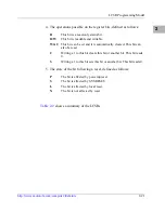
Requested Snoop Operation
10
9
MC68040
MC68060
0
0
Snoop disabled
Snoop enabled
0
1
Source dirty, sink byte/word/longword
Snoop disabled
1
0
Source dirty, invalidate line
Snoop enabled
1
1
Snoop disabled (Reserved)
Snoop disabled
Summary of Contents for MVME1X7P
Page 16: ...xvi ...
Page 18: ...xviii ...
Page 20: ...xx ...
Page 26: ...xxvi ...
Page 90: ...1 64 Computer Group Literature Center Web Site Programming Issues 1 ...
Page 248: ...3 50 Computer Group Literature Center Web Site PCCchip2 3 ...
Page 286: ...4 38 Computer Group Literature Center Web Site MCECC Functions 4 ...
Page 288: ...A 2 Computer Group Literature Center Web Site Summary of Changes A ...
Page 316: ...Index IN 14 Computer Group Literature Center Web Site I N D E X ...

