PCI Local Bus
http://www.motorola.com/computer/literature
1-29
1
Software Readable Header/Switch Register (S1)
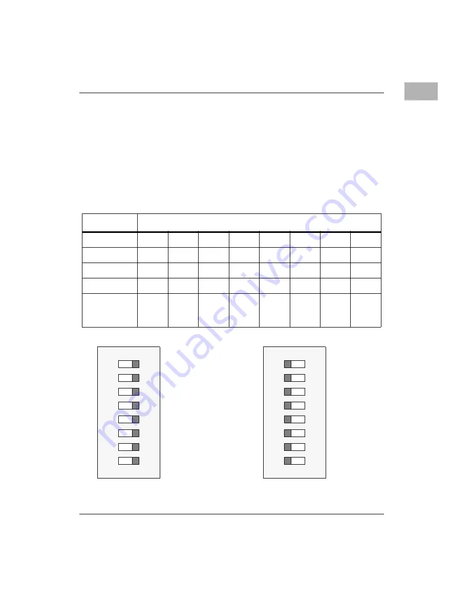
The MVME5100’s use of this register is fully compliant with the
PowerPlus II internal programming configuration. A 1x8 header/switch
(S1) is provided as the Software Readable Header/Switch (SRH). A logic
0 means the header/switch is in the "on" position for that particular bit and
a logic 1 means the header/switch is in the "off" position. SRH Register Bit
0 is associated with Pin 1 and Pin 16 of the SRH and SRH Register Bit 7
is associated with Pin 8 and Pin 9 of the SRH. The following table and
switch settings depict the aforementioned configuration.
REG
Software Readable Header/Switch Register - Offset 80E0h
BIT
RD0
RD1
RD2
RD3
RD4
RD5
RD6
RD7
FIELD
SRH7
SRH6
SRH5
SRH4
SRH3
SRH2
SRH1
SRH0
OPER
R
R
R
R
R
R
R
R
RESET
N/A
N/A
N/A
N/A
N/A
N/A
N/A
N/A
REQUIRED
OR
OPTIONAL
O
O
O
O
O
O
O
O
SRH0 = 0
SRH1 = 0
SRH2 = 0
SRH3 = 0
SRH4 = 0
SRH5 = 0
SRH6 = 0
SRH7 = 0
SRH0 = 1
SRH1 = 1
SRH2 = 1
SRH3 = 1
SRH4 = 1
SRH5 = 1
SRH6 = 1
SRH7 = 1
ON
ON
1
1
16
16
12345678
12345678
Summary of Contents for MVME5100 Series
Page 1: ...MVME5100 Single Board Computer Programmer s Reference Guide V5100A PG2 September 2001 Edition ...
Page 16: ...xvi ...
Page 20: ...xx ...
Page 28: ...xxviii ...
Page 62: ...1 34 Computer Group Literature Center Web Site Product Data and Memory Maps 1 ...
Page 278: ...3 88 Computer Group Literature Center Web Site System Memory Controller SMC 3 ...
Page 288: ...4 10 Computer Group Literature Center Web Site Hawk Programming Details 4 ...
Page 320: ...Index IN 12 Computer Group Literature Center Web Site I N D E X ...


