


Programming Model
http://www.motorola.com/computer/literature
3-59
3
Writes that change these bits must be enveloped by a
period of time in which no accesses to ROM/Flash Block
A, occur. A simple way to provide the envelope is to
perform at least two accesses to this or another of the
SMC’s registers before and after the write.
rom_b_spd0,1
rom_b_spd0,1 determine the access timing used for
ROM/Flash Block B. Refer to the table above.
Writes that change these bits must be enveloped by a
period of time in which no accesses to ROM/Flash, Bank
B, occur. A simple way to provide the envelope is to
perform at least two accesses to this or another of the
SMC’s registers before and after the write.
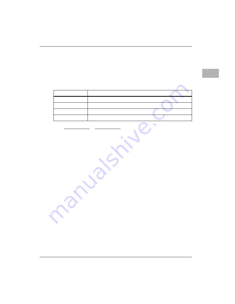
Table 3-15. ROM Speed Bit Encodings
rom_a/b_spd0,1
Approximate ROM Block A/B Device Access Time
%00
12 Clock Periods (120ns @ 100 MHz, 180ns @ 66.67 MHz)
%01
8 Clock Periods (80ns @ 100 MHz, 120ns @ 66.67 MHz)
%10
5 Clock Periods (50ns @ 100 MHz, 75ns @ 66.67 MHz)
%11
3 Clock Periods (30ns @100 MHz, 45ns @ 66.67 MHz)
Summary of Contents for MVME5100 Series
Page 1: ...MVME5100 Single Board Computer Programmer s Reference Guide V5100A PG2 September 2001 Edition ...
Page 16: ...xvi ...
Page 20: ...xx ...
Page 28: ...xxviii ...
Page 62: ...1 34 Computer Group Literature Center Web Site Product Data and Memory Maps 1 ...
Page 278: ...3 88 Computer Group Literature Center Web Site System Memory Controller SMC 3 ...
Page 288: ...4 10 Computer Group Literature Center Web Site Hawk Programming Details 4 ...
Page 320: ...Index IN 12 Computer Group Literature Center Web Site I N D E X ...


