Introduction
http://www.motorola.com/computer/literature
1-3
1
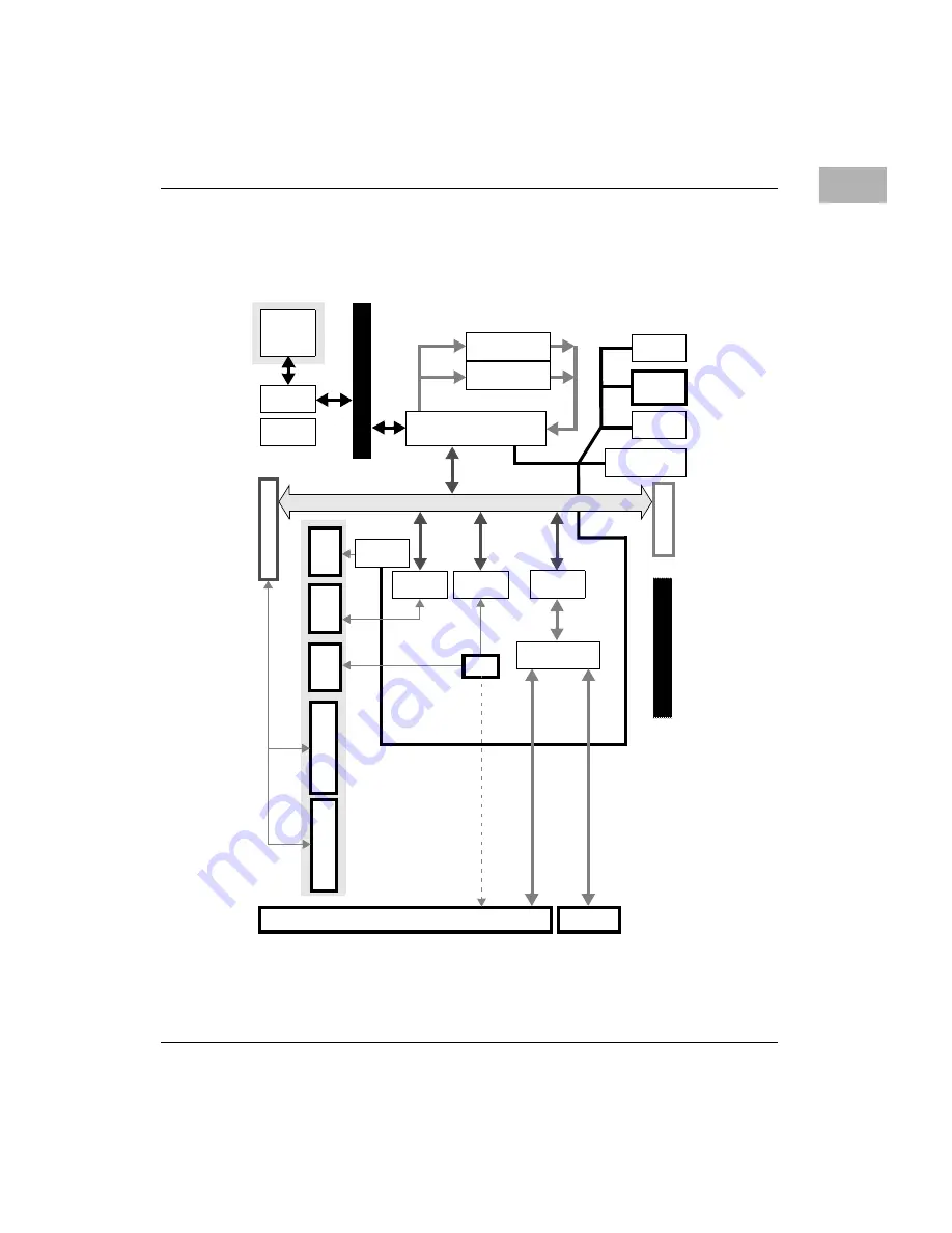
The following block diagram illustrates the architecture of the
MVME5100 Single Board Computer.
Figure 1-1. MVME5100 Block Diagram
Processor
750 Max
100 MHz
MP
C604 Pr
oces
sor
Bus
VME P1
PCI Expan
sion
System
Registers
FLASH
1MB to 17MB
Clock
Generator
VME Bridge
Universe 2
Ethernet 1
10/100TX
Buffers
RTC/NVRAM/WD
M48T37V
TL16C550
UART/9pin
Fr
o
n
t Pa
n
e
l
VME P2
RJ
4
5
PM
C
F
ront I/O
P
M
C Fr
ont I/O
SLot1
S
lot2
2,
64-bit
PM
C S
lots
L2 Cache
1M,2M
Ethernet 2
10/100TX
1
0
/100Tx
RJ
4
5
10/
100Tx
Hawk X-bus
RJ
4
5
DE
B
U
G
planar
761 or PMC
IP
MC
761 REC
EPT
AC
L
E
Mezzanine SDRAM
32MB to 512MB
SDRAM
32MB to 512MB
HDR
Hawk Asic
System Memory Controller (SMC)
and PCI Host Bridge (PHB)
TL16C550
UART
33 MHz 32/64-bit PCI Local Bus
Summary of Contents for MVME5100 Series
Page 1: ...MVME5100 Single Board Computer Programmer s Reference Guide V5100A PG2 September 2001 Edition ...
Page 16: ...xvi ...
Page 20: ...xx ...
Page 28: ...xxviii ...
Page 62: ...1 34 Computer Group Literature Center Web Site Product Data and Memory Maps 1 ...
Page 278: ...3 88 Computer Group Literature Center Web Site System Memory Controller SMC 3 ...
Page 288: ...4 10 Computer Group Literature Center Web Site Hawk Programming Details 4 ...
Page 320: ...Index IN 12 Computer Group Literature Center Web Site I N D E X ...


