


10
603 Hardware Specifications
1.4.2.3 Output AC Specifications
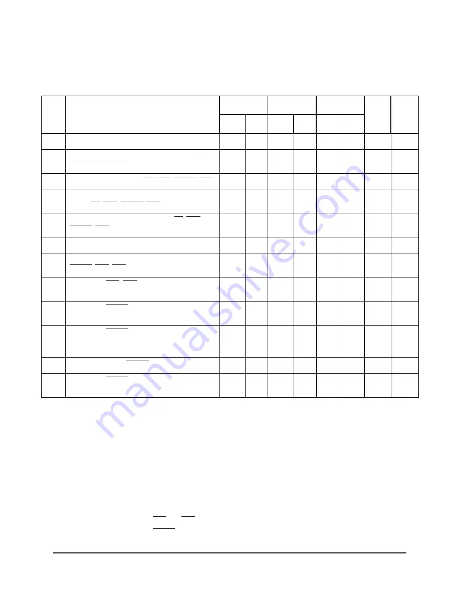
Table 8 provides the output AC timing specifications for the 603 as defined in Figure 4.
Table 8. Output AC Timing Specifications
1
Vdd = 3.3
±
5% V dc, GND = 0 V dc, CL = 50 pF, 0
≤
T
j
≤
105
°
C
Num
Characteristic
66C
66A
80C
Unit
Notes
Min
Max
Min
Max
Min
Max
12
SYSCLK to output driven (output enable time)
1.0
—
1.0
—
1.0
—
ns
13a
SYSCLK to output valid (5.5 V to 0.8 V— TS,
ABB, ARTRY, DBB)
—
13.0
—
10.0
—
12.0
ns
4
13b
SYSCLK to output valid (TS, ABB, ARTRY, DBB)
—
12.0
—
9.0
—
11.0
ns
6
14a
SYSCLK to output valid (5.5 V to 0.8 V— all
except TS, ABB, ARTRY, DBB)
—
15.0
—
12.0
—
14.0
ns
4
14b
SYSCLK to output valid (all except TS, ABB,
ARTRY, DBB)
—
13.0
—
10.0
—
12.0
ns
6
15
SYSCLK to output invalid (output hold)
1.5
—
1.5
—
1.5
—
ns
3
16
SYSCLK to output high impedance (all except
ARTRY, ABB, DBB)
—
11.5
—
8.5
—
10.5
ns
17
SYSCLK to ABB, DBB, high impedance after
precharge
—
1.0
—
1.2
—
1.0
t
sysclk
5,7
18
SYSCLK to ARTRY high impedance before
precharge
—
11.0
—
8.0
—
10.0
ns
19
SYSCLK to ARTRY precharge enable
0.2
*
t
sysclk
+ 1.0
—
0.2
*
t
sysclk
+ 1.0
—
0.2
*
t
sysclk
+ 1.0
—
ns
3,5,8
20
Maximum delay to ARTRY precharge
—
1.0
—
1.2
—
1.0
t
sysclk
5,8
21
SYSCLK to ARTRY high impedance after
precharge
—
2.0
—
2.25
—
2.0
t
sysclk
5,8
Notes:
1. All output specifications are measured from the 1.4 V of the rising edge of SYSCLK to the TTL level (0.8 V or 2.0 V)
of the signal in question. Both input and output timings are measured at the pin
2. All maximum timing specifications assume C
L
= 50 pF.
3. This minimum parameter assumes C
L
= 0 pF.
4. SYSCLK to output valid (5.5 V to 0.8 V) includes the extra delay associated with discharging the external voltage
from 5.5 V to 0.8 V instead of from Vdd to 0.8 V (5 V CMOS levels instead of 3.3 V CMOS levels).
5. t
sysclk
is the period of the external bus clock (SYSCLK) in nanoseconds (ns). The numbers given in the table must be
multiplied by the period of SYSCLK to compute the actual time duration (in nanoseconds) of the parameter in
question.
6. Output signal transitions from GND to 2.0 V or Vdd to 0.8 V.
7. Nominal precharge width for ABB and DBB is 0.5 t
sysclk
.
8. Nominal precharge width for ARTRY is 1.0 t
sysclk
.


