


603 Hardware Specifications
5
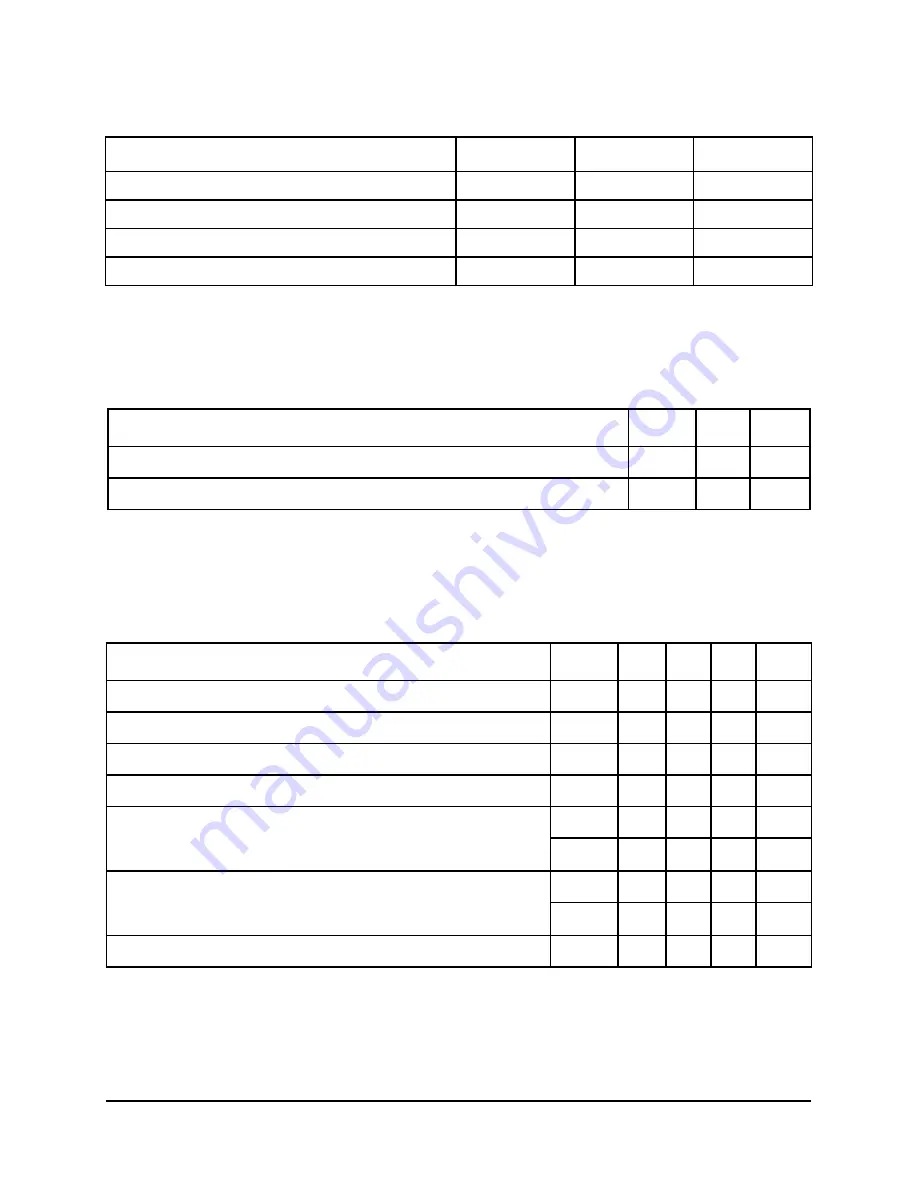
Table 2 provides the recommended operating conditions for the 603.
Table 3 provides the package thermal characteristics for the 603.
Table 4 provides the DC electrical characteristics for the 603.
Table 2. Recommended Operating Conditions
Characteristic
Symbol
Value
Unit
Core supply voltage
Vdd
3.135 to 3.465
V
PLL supply voltage
AVdd
3.135 to 3.465
V
Input voltage
V
in
–0.3 to 5.5
V
Die-junction temperature
T
j
0 to 105
°
C
Notes
: These are the recommended and tested operating conditions. Proper device operation outside of these
conditions is not guaranteed.
Table 3. Package Thermal Characteristics
Characteristic
Symbol
Value
Rating
Motorola wire-bond CQFP package die junction-to-case thermal resistance (typical)
θ
JC
2.2
°
C/W
IBM C4-CQFP package die junction-to-heat sink base thermal resistance (typical)
θ
JS
1.1
°
C/W
Note:
Refer to Section 1.8, “System Design Information,” for more details about thermal management.
Table 4. DC Electrical Specifications
Vdd = 3.3
±
5% V dc, GND = 0 V dc, 0
≤
T
j
≤
105
°
C
Characteristic
Symbol
Min
Max
Unit
Notes
Input high voltage (all inputs except SYSCLK)
V
IH
2.2
5.5
V
Input low voltage (all inputs except SYSCLK)
V
IL
GND
0.8
V
SYSCLK input high voltage
CV
IH
2.4
5.5
V
SYSCLK input low voltage
CV
IL
GND
0.4
V
Input leakage current, V
in
= 3.465 V
V
in
= 5.5 V
I
in
—
10
µ
A
1
I
in
—
TBD
µ
A
1
Hi-Z (off-state) leakage current, V
in
=
3.465 V
V
in
=
5.5
V
I
TSI
—
10
µ
A
1
I
TSI
—
TBD
µ
A
1
Output high voltage, I
OH
= –9
mA
V
OH
2.4
—
V


