


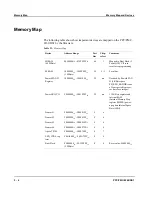

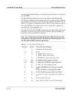
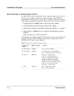
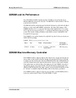
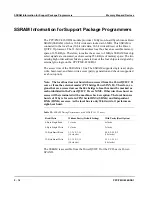
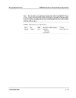
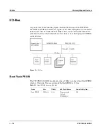
Memory Map and Devices
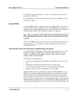
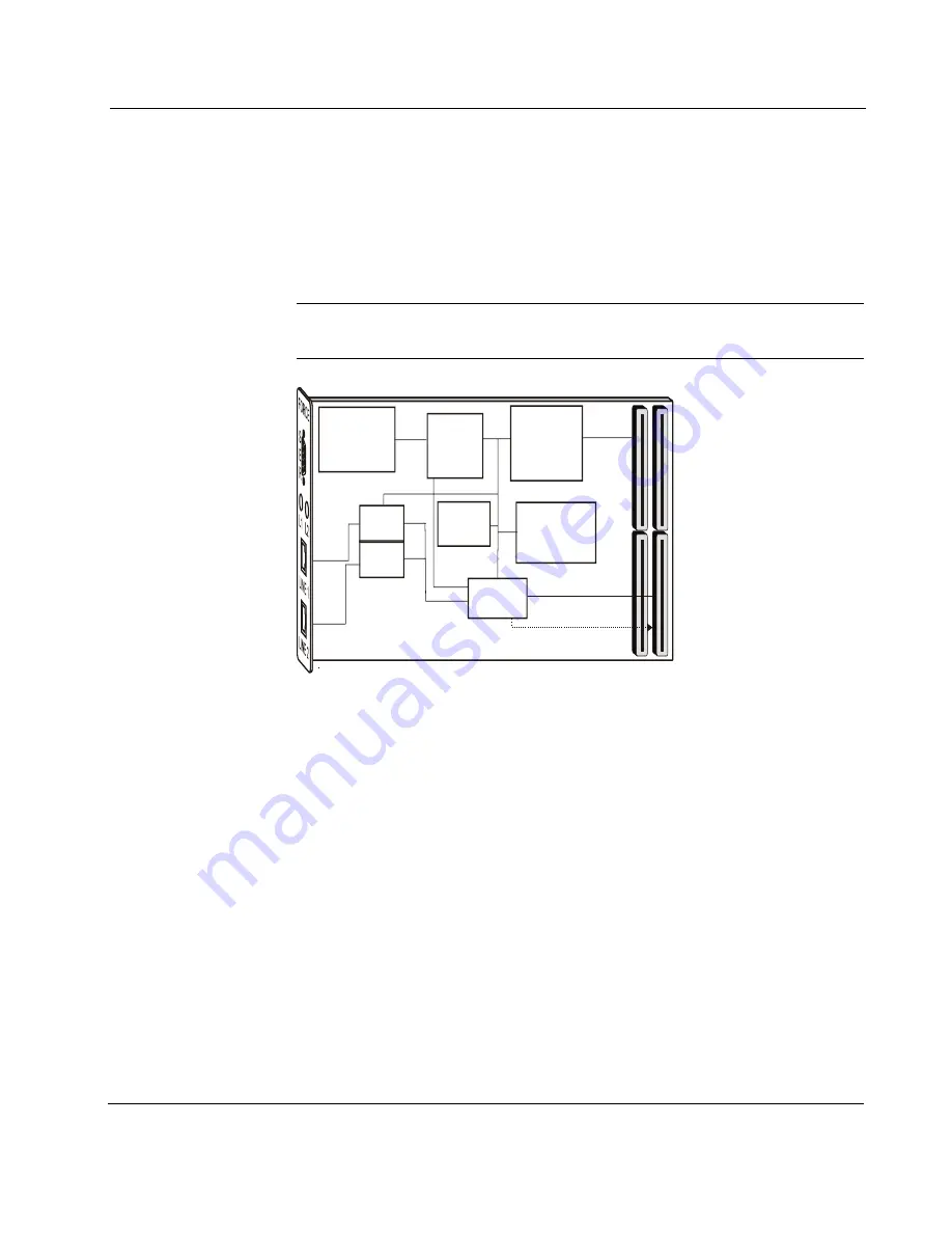
Block Diagram
PPC/PMC-8260/DS1
5 - 3
Block Diagram
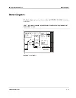
The block diagram gives an overview on how the PPC/PMC-8260/DS1 devices are
connected.
Note: The inter-TMD link represented as a dotted line is only available on
the H.110-F variant.
Tundra
PowerSPAN II
PCI Bridge
33/66 MHz
SDRAM 64 Bit
64 MByte
66 MHz
SSRAM 32 Bit
1 MByte
66 MHz
Boot Flash
2 MByte
Agere
T8105
H.110 or SCbus
Inter-TDM Link
Line 1
Line 2
Motorola
MPC8260
300 MHz
Framer
PM4351
Framer
PM4351
PCI Bus
32-/64 bit,
33/66MHz
60x
Bus
Local
Bus
Figure 14:
Block Diagram
Summary of Contents for PPC/PMC-8260/DS1
Page 1: ...PPC PMC 8260 DS1 Reference Guide P N 6806800B10A July 2006 ...
Page 8: ...viii PPC PMC 8260 DS1 ...
Page 22: ...xxii PPC PMC 8260 DS1 ...
Page 26: ...xxvi PPC PMC 8260 DS1 ...
Page 30: ...xxx PPC PMC 8260 DS1 ...
Page 31: ...1 Introduction ...
Page 32: ......
Page 39: ...2 Installation ...
Page 40: ......
Page 53: ...3 Indicators and Connectors ...
Page 54: ......
Page 64: ...On Board Connectors Indicators and Connectors 3 12 PPC PMC 8260 DS1 ...
Page 65: ...4 Firmware ...
Page 66: ......
Page 104: ...Code Examples Firmware 4 40 PPC PMC 8260 DS1 ...
Page 105: ...5 Memory Map and Devices ...
Page 106: ......
Page 132: ...Resetting the Devices Memory Map and Devices 5 28 PPC PMC 8260 DS1 ...
Page 133: ...6 TDM Channel Configuration ...
Page 134: ......
Page 145: ...A Troubleshooting ...
Page 146: ......
Page 148: ...A 4 PPC PMC 8260 DS1 ...
Page 150: ...I 2 PPC PMC 8260 DS1 ...


