


Synchronizing the Clock
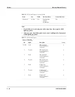
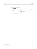
TDM Channel Configuration
6 - 4
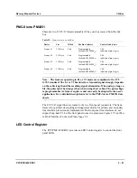
PPC/PMC-8260/DS1
Synchronizing the Clock
If the devices in a telecommunication network use different clocks, you will not be
able to operate your network. To be able to create a synchronuous network in
which all devices use the same clock, the Agere T8105 switch includes a clock
multiplexer to select among the possible sources. It is possible to configure the
PPC/PMC-8260/DS1 to be the clock slave or the clock master.
There may be more ways to configure the clocks than described in this section. For
further information, refer to the T8105 documentation.
Configuring the PPC/PMC-8260/DS1 as Clock Master
If the PPC/PMC-8260/DS1 is to be configured as clock master, the following on-
board sources can be used to provide the master clock:
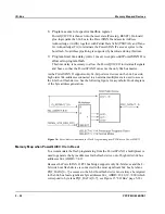
•
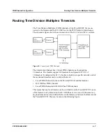
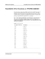
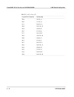
Line recovered network reference of one of the framers which are provided to
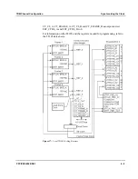
the T8105 on its L_REF[0:3] pins. Figure 17 “Local TDM Clocking Structure”
on page 6-5 shows which framer is connected to which L_REF pin.
•
On-board 8 kHz clock (+/- 50ppm) connected to L_REF_5 of T8105
•
On-board quarz crystal oscillator clock 16.384 MHz (+/- 10ppm) which is pro-
vided via the T8105 XTALIN/XTALOUT pins.
•
CTBus network reference clocks CT_NETREF_1 and CT_NETREF_2 (see
Figure 17 “Local TDM Clocking Structure” on page 6-5).
To use one of these clocks, select one of the L_REF input pins, the quarz oscillator
input pin, or the CT_NETREF_x input pins inside the T8105 switch via T8105 reg-
isters. The selected clocks are then distributed via frame pulse clock line L_SC_1
and bit clock line TCLK_OUT and a clock driver to the clock lines of the framers
(BTCLK, BTFP) and the PowerQUICC II (L1RCLK and L1RSYNC). In this way,
all on-board devices use the same clock. Figure 17 “Local TDM Clocking Struc-
ture” on page 6-5 shows the clock driver and the clock lines.
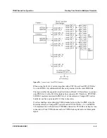
The PPC/PMC-8260/DS1 can be configured as primary or secondary H.110 bus
clock master. In order to do this, program CT_C8_A and CT_FRAME_A or
CT_C8_B and CT_FRAME_B inside the T8105 as output.
When operating as H.110 bus clock master and driving CT_C8_A and
CT_FRAME_A or CT_C8_B and CT_FRAME_B according to the H.110 bus
specification, clock masters must shortcut the 33 Ohm series termination resistors
available in the signals CT_C8_A and CT_FRAME_A or CT_C8_B and
CT_FRAME_B. On the PPC/PMC-8260/DS1, this can be accomplished via the
T8105 general purpose I/O pins GP(0)=FET_CTRL_A and GP(0)=FET_CTRL_B.
Normally, these GPIO pins are configured as inputs, so that you have to program
Summary of Contents for PPC/PMC-8260/DS1
Page 1: ...PPC PMC 8260 DS1 Reference Guide P N 6806800B10A July 2006 ...
Page 8: ...viii PPC PMC 8260 DS1 ...
Page 22: ...xxii PPC PMC 8260 DS1 ...
Page 26: ...xxvi PPC PMC 8260 DS1 ...
Page 30: ...xxx PPC PMC 8260 DS1 ...
Page 31: ...1 Introduction ...
Page 32: ......
Page 39: ...2 Installation ...
Page 40: ......
Page 53: ...3 Indicators and Connectors ...
Page 54: ......
Page 64: ...On Board Connectors Indicators and Connectors 3 12 PPC PMC 8260 DS1 ...
Page 65: ...4 Firmware ...
Page 66: ......
Page 104: ...Code Examples Firmware 4 40 PPC PMC 8260 DS1 ...
Page 105: ...5 Memory Map and Devices ...
Page 106: ......
Page 132: ...Resetting the Devices Memory Map and Devices 5 28 PPC PMC 8260 DS1 ...
Page 133: ...6 TDM Channel Configuration ...
Page 134: ......
Page 145: ...A Troubleshooting ...
Page 146: ......
Page 148: ...A 4 PPC PMC 8260 DS1 ...
Page 150: ...I 2 PPC PMC 8260 DS1 ...


