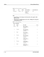
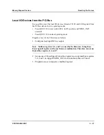


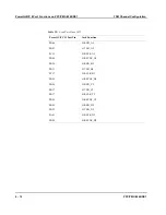


Synchronizing the Clock
TDM Channel Configuration
6 - 6
PPC/PMC-8260/DS1
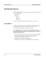
Configuring the PPC/PMC-8260/DS1 as Clock Slave
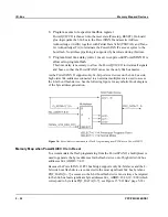
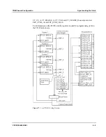
Depending on which clock line (A or B) is the H.110 bus master clock line, pro-
gram CT_C8_A or CT_C8_B and CT_FRAME_A or CT_FRAME_B inside the
T8105 as input. The clocks are then distributed via frame pulse clock line L_SC_1
and bit clock line TCLK_OUT and a clock driver to the clock lines of the framers
(BTCLK, BTFP) and the PowerQUICC II (L1RCLK and L1RSYNC). Figure 17
“Local TDM Clocking Structure” on page 6-5 shows these clock lines.
The T8105 general purpose I/O pins FET_CTRL_A and FET_CTRL_B must be
configured to activate the 33 Ohm series resistors of line A and B. This is accom-
plished by setting the bits FET_CTRL_A and FET_CTRL_B to 1 (default).
For information on the T8105 and the registers needed for programming, refer to
the T8105 data sheets.
Summary of Contents for PPC/PMC-8260/DS1
Page 1: ...PPC PMC 8260 DS1 Reference Guide P N 6806800B10A July 2006 ...
Page 8: ...viii PPC PMC 8260 DS1 ...
Page 22: ...xxii PPC PMC 8260 DS1 ...
Page 26: ...xxvi PPC PMC 8260 DS1 ...
Page 30: ...xxx PPC PMC 8260 DS1 ...
Page 31: ...1 Introduction ...
Page 32: ......
Page 39: ...2 Installation ...
Page 40: ......
Page 53: ...3 Indicators and Connectors ...
Page 54: ......
Page 64: ...On Board Connectors Indicators and Connectors 3 12 PPC PMC 8260 DS1 ...
Page 65: ...4 Firmware ...
Page 66: ......
Page 104: ...Code Examples Firmware 4 40 PPC PMC 8260 DS1 ...
Page 105: ...5 Memory Map and Devices ...
Page 106: ......
Page 132: ...Resetting the Devices Memory Map and Devices 5 28 PPC PMC 8260 DS1 ...
Page 133: ...6 TDM Channel Configuration ...
Page 134: ......
Page 145: ...A Troubleshooting ...
Page 146: ......
Page 148: ...A 4 PPC PMC 8260 DS1 ...
Page 150: ...I 2 PPC PMC 8260 DS1 ...


