


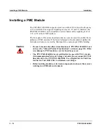


Requirements
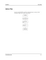
Installation
2 - 4
PPC/PMC-8260/DS1
Requirements
The installation requires:
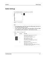
•
Backplane according to used carrier board:
– CompactPCI carrier board: CompactPCI (optional CompactPCI-H.110)
backplane system with power supply
– VMEbus carrier board: VMEbus (optional VMEbus-SCbus) backplane sys-
tem with power supply
•
Corresponding carrier board with at least one PMC slot
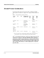
Long Haul Requirements
The two front-panel line interfaces in T1 mode on the SC-F and H.110-F variants
are DSX-1 type interfaces which means that in T1 mode, the interfaces do not sup-
port long haul required for public networks. To be able to operate the PPC/PMC-
8260/DS1 in a public network you need a CSU (channel service unit).
Carrier Board Signaling Level Requirements
The PPC/PMC-8260/DS1 supports signaling levels 3.3V and 5V and therefore is a
universal PMC module. Make sure that your carrier board has a signaling level of
3.3V or 5V at the PMC interface.
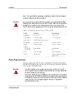
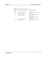
Environmental Requirements
The environmental values given in the table below must be tested and proven in the
used system configuration. Operating temperatures refer to the temperature of the
air circulating around the board and not to the actual component temperature.
Summary of Contents for PPC/PMC-8260/DS1
Page 1: ...PPC PMC 8260 DS1 Reference Guide P N 6806800B10A July 2006 ...
Page 8: ...viii PPC PMC 8260 DS1 ...
Page 22: ...xxii PPC PMC 8260 DS1 ...
Page 26: ...xxvi PPC PMC 8260 DS1 ...
Page 30: ...xxx PPC PMC 8260 DS1 ...
Page 31: ...1 Introduction ...
Page 32: ......
Page 39: ...2 Installation ...
Page 40: ......
Page 53: ...3 Indicators and Connectors ...
Page 54: ......
Page 64: ...On Board Connectors Indicators and Connectors 3 12 PPC PMC 8260 DS1 ...
Page 65: ...4 Firmware ...
Page 66: ......
Page 104: ...Code Examples Firmware 4 40 PPC PMC 8260 DS1 ...
Page 105: ...5 Memory Map and Devices ...
Page 106: ......
Page 132: ...Resetting the Devices Memory Map and Devices 5 28 PPC PMC 8260 DS1 ...
Page 133: ...6 TDM Channel Configuration ...
Page 134: ......
Page 145: ...A Troubleshooting ...
Page 146: ......
Page 148: ...A 4 PPC PMC 8260 DS1 ...
Page 150: ...I 2 PPC PMC 8260 DS1 ...


