6
STARLINE
RF Amplifier Quick Start Guide
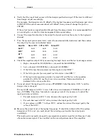
ADU Pads and Levels
A JXP pad is installed in the input line to the ADU location. This pad adjusts the ADU input
level for the standard application of the amplifier. This pad may be changed depending on the
operational output of the amplifier.
In general, the following JXP pad values are recommended in the amplifier ADU circuit and are
the standard values installed at the factory.
Amplifier
Pad
Amplifier Output Level Range
BLE*/*
JXP-6
+
42 dBmV to
+
50 dBmV at 550 MHz
MB*/*
JXP-14
+
42 dBmV to
+
50 dBmV at 550 MHz
BT*/*
JXP-6
+
41 dBmV to
+
51 dBmV at 550 MHz
MBE*/*
JXP-0 or
JXP-ZX jumper
+
31 dBmV to
+
38 dBmV (trunk) and
+
40 dBmV to
+
47 dBmV (bridger) at 550 MHz
To determine the correct ADU pad value for other output levels:
!
Increase the ADU pad by 1 dB for every 1 dBmV increase in output level.
!
Decrease the ADU pad by 1 dB for every 1 dBmV decrease in output level.
The levels for the MBE
*
/
*
assume a bridger gain 9 dB higher than the trunk.
Return Path Alignment
The following subsections describe procedures required to obtain proper return path alignment.
Before You Begin
For proper return path alignment obtain:
1
RF alignment levels and insertion points for all amplifiers
2
RF reference output level of the headend optical receivers
3
A full complement of JXP-
*
B pads and SRE-
*
-
*
return equalizers
4
A reverse signal generator that produces at least one signal within the return bandpass and
has a variable output
5
Return sweep or alignment equipment
It is recommended that you:
1
Do not use wire jumpers to bypass the SRE-
*
-
*
location.
2
Set up the return optical link before you perform the amplifier set up.
3
Specify reverse alignment design levels for a single carrier.
4
Consider sweep equipment as a single carrier and operate at design levels.
5
Do not include injection point losses in reverse design levels.
If JXP THERM devices (JXP-TH
*
B) are specified for level control, they need to be installed in
the JXP THERM pad facility.


