Overview 2-7
PRELIMINARY - Motorola Internal Use Only
SLE*-* Installation and Operation Manual
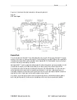
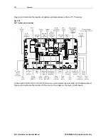
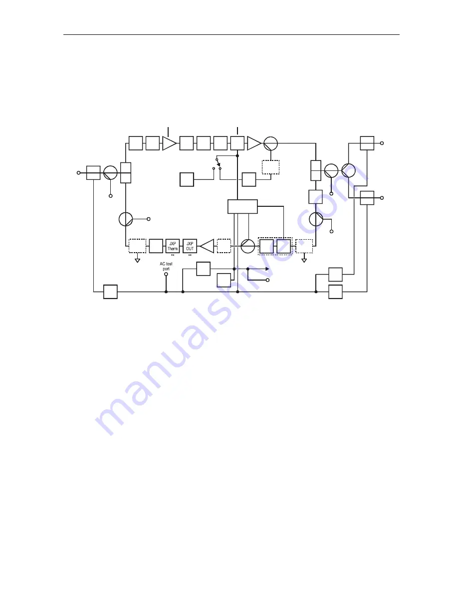
Figure 2-7 illustrates the interconnection of these components:
Figure 2-7
SLE*-* block diagram
Input
port
Output
port 1
Output
port 2
**
RTN
EQ
-16 dB
LPF
-20 dB
TP
-20 dB
TP
-20 dB
TP
-20 dB
TP
**
**
**
**
ICS
JXP
JXP
IN
H
L
24 Vdc
DC test port
Power
supply
Fuse
Fuse
Fuse
** Plug-in module
Surge
protector
Surge
protector
Pilot
filter
-1.0 dB
-1.0 dB
-0.8 dB
-0.0 dB
-0.0 dB
0.0 dB
25 dB
PP
-0.4 dB
-0.4 dB
0.0 dB
-0.4 dB
RF
AC
-0.5 dB
-0.5 dB
-4.0 dB
-0.5 dB
-0.5 dB
-4.0 dB
**
**
**
**
**
**
**
**
**
JXP
IN
FWD
EQ
JXP
MID 1
JXP
MID 2
Bode
PP
PD
MGC
**
LDR
Manual
Auto
Auto
-1.0 dB
18.5 dB for SLE 87*-X
24 dB for SLE 87*-H
23 dB
0.0 dB with jumper
(7.0 dB w/Bode)
-1.0 dB
-5.0 dB
-5.0 dB
0.0 dB
0.0 dB
0.0 dB
AGC
**
STATUS
MONITOR PIN
H
L
-1.0 dB
-1.0 dB
RF
AC
RF
AC
TVS
Return Path
The circuit board of the SLE*-* accommodates the return path. This equips the SLE*-* to pass
signals in the return or upstream direction. The standard circuit board contains all components
including the diplex filters with extended return bandwidth for the amplifier input and output.
All items are plug-in and easily installed.
Optional SRE-*-* return equalizers compensate for cable attenuation and are available in 1 dB
increments for S-split, and 2 dB increments for all other splits, from 0 dB through 12 dB.
The input and output of the return path each include a JXP-*B pad facility. You can also use
either pad socket as a test point or a signal injection point. The return output pad value is
normally selected to control the return signal level into the next upstream amplifier. Select an
appropriate return input pad to attenuate excessive input signal.
The return-input test point and the return-output test point are
−
20 dB directional couplers.
Both test points present 75-ohm source impedance and do not require special test probes.


