Amplifier
Setup
3-13
PRELIMINARY - Motorola Internal Use Only
SLE*-* Installation and Operation Manual
It is recommended that you:
!
Do not use wire jumpers to bypass the SRE-*-* location.
!
Perform the return optical link setup before performing amplifier setup.
!
Specify reverse alignment design levels for a single carrier.
!
Consider sweep equipment as a single carrier and operate at design levels.
!
Do not include injection point losses in reverse design levels.
If JXP THERM devices (JXP-TH*C) are specified for level control, they should be installed in
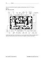
the JXP THERM pad facility (illustrated in Figure 2-8).
Alignment Procedure
The return amplifier configuration includes one standard-gain (25 dB) return amplifier hybrid
and an appropriate SRE-*-* equalizer. All components are plug-in and are easily installed.
To align the return path:
1
If the SLE*-* is powered, remove all fuses before you perform the following steps.
2
Install the design value pad in the return output pad location (
JXP OUT
).
3
Install the design value return equalizer in the SRE-*-* location.
4
Verify that the return input pad location (
JXP
-
IN
) has a 0 dB pad (or JXP-ZX jumper)
installed.
5
If you ordered the optional ICS, verify that the switch is installed in the ICS location. If it
was not ordered, the factory-installed jumper should remain in the ICS location.
6
Verify that the return output pad socket (JXP THERM), located between the hybrid output
and the SRE-*-*, has a 0 dB pad (or JXP-ZX jumper) or a JXP-TH*C installed.
7
Set the sweep equipment output level to the amplifier’s design input level. Add insertion
point loss.
8
If required, change the return output pad (
JXP OUT
) and/or return equalizer to achieve, as
closely as possible, a match of the reference level as compared to the node.
9
Verify the sweep response of all insertion points if applicable.
10
Verify that the pad and equalizer values are similar to the map design values.
You can verify proper return alignment by injecting a carrier, at the design level, into any
amplifier at random. Proper alignment is achieved if you observe the reference level at the
headend optical receiver output.
Return levels used for alignment are not necessarily operational system levels. These levels
vary from system to system due to differences in equipment, architectures, and design
philosophies. For an in-depth analysis and discussion of the return path, refer to Motorola
reference guide Return Path Level Selection, Setup, and Alignment Procedure.


