background image

ii

Manual Rev: 1.0

Release Date: August 2004

FCC-B Radio Frequency Interference Statement

This equipment has been tested and found to comply with the limits for a class B

digital device, pursuant to part 15 of the FCC rules. These limits are designed to

provide reasonable protection against harmful interference when the equipment is

operated in a commercial environment. This equipment generates, uses and can

radiate radio frequency energy and, if not installed and used in accordance with the

instruction manual, may cause harmful interference to radio communications. Opera-

tion of this equipment in a residential area is likely to cause harmful interference, in

which case the user will be required to correct the interference at his own expense.

Notice 1

The changes or modifications not expressly approved by the party responsible for

compliance could void the user’s authority to operate the equipment.

Notice 2

Shielded interface cables and A.C. power cord, if any, must be used in order to

comply with the emission limits.

VOIR LA NOTICE D’INSTALLATION AVANT DE RACCORDER AU RESEAU.

Micro-Star International

MS-7067

This device complies with Part 15 of the FCC Rules. Operation is subject to the

following two conditions:

(1) this device may not cause harmful interference, and

(2) this device must accept any interference received, including interference that may

cause undesired operation.

Summary of Contents for MS-7067

Page 1: ...i MS 7067 v1 X Micro ATX Mainboard English Version G52 M7067X1...

Page 2: ...ment in a residential area is likely to cause harmful interference in which case the user will be required to correct the interference at his own expense Notice 1 The changes or modifications not expr...

Page 3: ...2003 NT XP are registered trademarks of Microsoft Corporation Netware is a registered trademark of Novell Inc Award is a registered trademark of Phoenix Technologies Ltd AMI is a registered trademark...

Page 4: ...or module 9 All cautions and warnings on the equipment should be noted 10 Never pour any liquid into the opening that could damage or cause electrical shock 11 If any of the following situations arise...

Page 5: ...to LGA 775 CPU 2 5 CPU Cooler Installation 2 5 Memory 2 8 DDR Module Combination 2 8 Installing DDR Modules 2 8 Power Supply 2 9 ATX 20 Pin Power Connector ATX1 2 9 ATX 12V Power Connector JPW1 2 9 B...

Page 6: ...I2C Optional 2 17 IEEE 1394 Connector J1394_1 F1_1394 Optional 2 17 Jumper 2 18 BIOS Flash Jumper BIOS_WP Optional 2 18 Clear CMOS Jumper CLR_CMOS 2 18 AGP Accelerated Graphics Port Slot 2 19 PCI Per...

Page 7: ...mainboard The MS 7067 mainboard is based on Intel 848P North Bridge ICH5 South Bridge chipsets for optimal system efficiency Designed to fit the advanced Intel Pentium 4 processors in Socket LGA775 th...

Page 8: ...er management Main Memory h Supports four memory banks using two 184 pin DDR DIMMs h Supports up to 2GB DDR400 333 266 SDRAMs without ECC For the updated supporting memory modules please visit http ww...

Page 9: ...ek 8110S Realtek 8100 C Integrated Fast Ethernet MAC and PHY in one chip Supports 10 100Mb s for 8100C and 10 100 1000Mb s for 8110S auto negotiation operation Compliant with PCI v2 2 and LAN on Mothe...

Page 10: ...keyboard T Line Out B Mic Line In M F_AUDIOJAUD1 BIOS_WP CD_IN Codec V IA VT6307 RT L8100C BAT1 Winbond W83627T HF Intel ICH5 IDE1 IDE2 FDD PCI1 PCI2 PCI3 FRISW IRDA PWR_FAN CPU_FAN SYS_FAN F_PANEL JP...

Page 11: ...up procedures While doing the installation be careful in holding the components and follow the installation procedures For some components if you install in the wrong orientation the compo nents will...

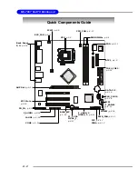
Page 12: ...p 2 11 FDD p 2 11 IDE1 IDE2 p 2 12 F_USB1 2 JUSB1 2 p 2 15 JAUD1 p 2 16 JPW1 p 2 9 CD_IN p 2 12 Back Panel I O p 2 10 ATX1 p 2 9 F_AUDIO p 2 16 SYS_FAN p 2 11 SATA2 1 p 2 14 JFP1 F_PANEL p 2 13 AGP S...

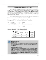
Page 13: ...p Example of CPU Core Speed Derivation Procedure If CPU Clock 200MHz Core Bus ratio 12 then CPU core speed Host Clock x Core Bus ratio 200MHz x 12 2 4 GHz Memory Speed CPU FSB Support Matrix MSI Remin...

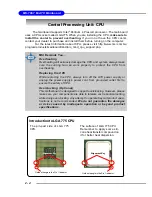
Page 14: ...from overheating Replacing the CPU While replacing the CPU always turn off the ATX power supply or unplug the power supply s power cord from grounded outlet first to ensure the safety of CPU Overcloc...

Page 15: ...talling the CPU make sure the CPU has a cooler at tached on the top to prevent overheating If you do not have the cooler contact your dealer to purchase and install them before turning on the computer...

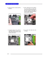
Page 16: ...frame Be sure to grasp on the edge of the CPU base Note that the align ment keys are matched 8 Cover the load plate onto the package 7 Visually inspect if the CPU is seated well into the socket If no...

Page 17: ...lightly onto the load plate and then se cure the lever with the hook under retention tab locking switch MSI Reminds You 1 Confirm if your CPU cooler is firmly installed before turning on your system...

Page 18: ...der You can install either single or double sided modules to meet your own needs Memory modules can be installed in any combination as follows S Single Side D Double Side The mainboard provides 2 slot...

Page 19: ...t to the ATX power supply make sure the plug of the power supply is inserted in the proper orientation and the pins are aligned Then push down the power supply firmly into the connector ATX 12V Power...

Page 20: ...Used 5 NC Not Used 6 RDN Receive Differential Pair 7 NC Not Used 8 NC Not Used Mouse Parallel Keyboard COM1 USB Ports L In MIC L Out LAN PIN SIGNAL 1 DCD 2 SIN 3 SOUT 4 DTR 5 GND 6 DSR 7 RTS 8 CTS 9 R...

Page 21: ...connecting the wire to the connectors always note that the red wire is the positive and should be connected to the 12V the black wire is Ground and should be connected to GND If the mainboard has a S...

Page 22: ...should always be connected to IDE1 IDE1 can connect a Master and a Slave drive You must configure second hard drive to Slave mode by setting the jumper accordingly IDE2 Secondary IDE Connector IDE2 ca...

Page 23: ...h reference pull up 7 RST_SW_P Reset Switch high reference pull up 8 PWR_SW_N Power Switch low reference pull down to GND 9 RSVD_DNU Reserved Do not use JFP1 Pin Definition JFP1 1 2 9 10 HDD LED Reset...

Page 24: ...subsystems Both connectors support 1st generation serial ATA data rate of 150 MB s and are fully compliant with Serial ATA 1 0 specifications Connect to SATA1 or SATA2 Take out the dust cover and conn...

Page 25: ...dy 7 RTS Request To Send 8 CTS Clear To Send 9 RI Ring Indicate Pin Definition COM2 1 2 9 9 2 JUSB1 2 1 10 Pin Description Pin Description 1 VCC 2 GND 3 USB0 4 Key 5 USB0 6 USB1 7 Key 8 USB1 9 GND 10...

Page 26: ...5VSB PS ON 1 Pin Description Pin Description 1 MIC 2 GND MIC 3 Front Line Out R 4 Line Next R 5 Front Line Out L 6 Line Next L 7 GND 8 Key F_AUDIO Pin Definition F_AUDIO 1 2 7 8 JAUD1 1 2 9 10 PIN SIG...

Page 27: ...ard provides optional IEEE 1394 pinheaders that allow you to con nect optional IEEE 1394 ports PIN SIGNAL PIN SIGNAL 1 TPA 2 TPA 3 Ground 4 Ground 5 TPB 6 TPB 7 Cablepower 8 Cablepower 9 Key no pin 10...

Page 28: ...cannot be updated Clear CMOS Jumper CLR_CMOS There is a CMOS ROM onboard that has a power supply from external battery to keep the data of system configuration With the CMOS ROM the system can automat...

Page 29: ...ou to insert expansion cards to meet your needs When adding or removing expansion cards make sure that you unplug the power supply first Meanwhile read the documentation for the expansion card to make...

Reviews: