background image

2-10

MS-9803  Mainboard

Connector

IDE Connector: IDE1

This connector supports IDE hard disk drives, optical disk drives and other IDE devices.

Important

If you install two IDE devices on the same cable, you must configure the drives
separately  to master / slave mode by  setting  jumpers. Refer  to IDE  device

s

documentation supplied by the vendors for  jumper setting  instructions.

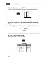
Chassis Intrusion Connector: JCASE1

This  connector  connects  to  the chassis intrusion switch  cable. If  the  chassis  is
opened, the chassis intrusion mechanism will be activated. The  system will record
this status and show a warning message on the screen. To clear the warning, you
must enter the BIOS utility and clear the record.

JCASE1

2

G

N

D

C

IN

T

R

U

1

IDE1

Summary of Contents for MS-9803

Page 1: ...i MS 9803 V1 X Mainboard G52 98031X3 Fuzzy GM965 GME965...

Page 2: ...ther countries PS 2 and OS 2 are registered trademarks of International Business Machines Corporation Windows 95 98 2000 NT XP are registered trademarks of Microsoft Corporation Netware is a registere...

Page 3: ...inserting any add on card or module 9 All cautions and warnings on the equipment should be noted 10 Never pour any liquid into the opening that could damage or cause electrical shock 11 If any of the...

Page 4: ...interference by one or more of the measures listed below Reorient or relocate the receiving antenna Increase the separation between the equipment and receiver Connect the equipment into an outlet on...

Page 5: ...v WEEE Waste Electrical and Electronic Equipment Statement...

Page 6: ...vi...

Page 7: ...vii...

Page 8: ...Layout 1 5 Board Dimension 1 6 Back Panel I O Shield Drawing 1 7 Power Consumption 1 8 Safety Compliance MTBF 1 9 Chapter 2 Hardware Setup 2 1 Quick ComponentsGuide 2 2 CPU Central Processing Unit 2...

Page 9: ...stem efficiency the Fuzzy GM965 GME965 accommodates the latest Intel Core 2 Duo Core Duo Celeron M processors in Socket P and supports two 240 pin 533 667MHz DDR2 DIMM slots to provide the maximum of...

Page 10: ...l ICH8M chipset Memory DDR2 533 667 SDRAM 4GB Max 2 DDR2 DIMM slots 240pin 1 8V LAN Supports 2 Gb Ethernet by Intel 82573L 82566DC Audio HDA Codec by Realtek ALC888 7 1 channel Compliant with Azalia 1...

Page 11: ...al I O connector 16GPIO 1 serial port connector 1 front panel connector 1 amplifier connector 4 pin Slots 1 PCI Express x16 slot 1 Mini PCI E slot 1 32 bit 33MHz PCI slot 1 CF socket optional Form Fac...

Page 12: ...MS 9803 Mainboard 1 4 Block Diagram...

Page 13: ...2 CON1 PCI1 J4 J7 J6 J5 JSPI2 JSPD1 ALC888 Intel 82573L Intel 82566DC JLPC1 JFP1 COM2 JLPT1 IDE1 SATA2 SATA1 ATX1 JAMP1 PCI E1 BATT Top Mouse Bottom Keyboard Top LAN Jack Bottom USB Ports Top LAN Jack...

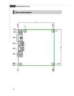
Page 14: ...MS 9803 Mainboard 1 6 Board Dimension...

Page 15: ...1 7 Product Overview Back Panel I O Shield Drawing...

Page 16: ...78 1 76 1 58 1 56 0 0 08 0 080 0 02 Windows Desktop Standby S3 with without two LANs connected stable 0 0 0 0 0 45 0 44 0 Windows Desktop Hibernate S4 with without two LANs connected stable 0 0 0 0 0...

Page 17: ...fication Title of standard EN 55022 1998 A1 2000 A2 2003 Class B Product family standard EN 6100 3 2 2000 Class D Limits for harmonic current emission EN 6100 3 3 1995 A1 2001 Limitation of voltage fl...

Page 18: ...MS 9803 Mainboard 1 10...

Page 19: ...dures While doing the installation be careful in holding the components and follow the installation procedures For some components if you install in the wrong orientation the components will not work...

Page 20: ...JCF_SEL1 p 2 20 JCASE1 p 2 10 JBAT1 p 2 18 Back Panel I O p 2 8 CPUFAN1 p 2 13 JFP1 p 2 13 PCI Slot p 2 19 F_USB1 2 p 2 16 PCI E Slot p 2 19 JLVDS1 p 2 15 SATA1 2 p 2 11 ATX1 p 2 7 JAMP1 p 2 12 JLPT1...

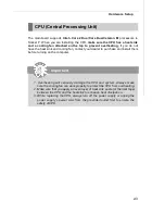
Page 21: ...ce heat dissipation 3 While replacing the CPU always turn off the power supply or unplug the power supply s power cord from the grounded outlet first to ensure the safety of CPU The mainboard supports...

Page 22: ...ush the CPU down until its pins securely fit into the socket CPU Cooler Installation for Socket P 4 On the front end of the CPU socket is a locking mechanism designed into the form of a screw head Mak...

Page 23: ...screw holes around the CPU socket where the CPU cooler backplate was installed Align the cooler set with the screw holes and mount it on top of the CPU 10 Connect the fan power cable to the CPUFAN1 co...

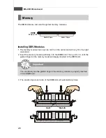
Page 24: ...ot Then push it in until the golden finger on the memory module is deeply inserted in the DIMM slot 3 The plastic clip at each side of the DIMM slot will automatically close Important You can barely s...

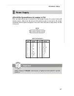
Page 25: ...18 5V 19 5V 20 5V PIN SIGNAL 1 3 3V 2 3 3V 3 GND 4 5V 5 GND 6 5V 7 GND 8 PW_OK 9 5V_SB 10 12V ATX 20 Pin System Power Connector ATX1 This connector allows you to connect to an ATX power supply To conn...

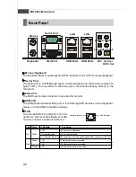
Page 26: ...ector is for a PS 2 mouse keyboard Serial Port The serial port is a 16550A high speed communications port that sends receives 16 bytes FIFOs You can attach a serial mouse or other serial devices direc...

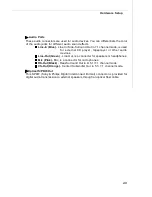
Page 27: ...CD player tapeplayer or other audio devices Line Out Green Line Out is a connector for speakers or headphones Mic Pink Mic is a connector for microphones RS Out Black Rear Surround Out in 4 5 1 7 1 ch...

Page 28: ...by setting jumpers Refer to IDE device s documentation supplied by the vendors for jumper setting instructions ChassisIntrusion Connector JCASE1 This connector connects to the chassis intrusion switc...

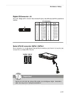
Page 29: ...gle Otherwise data loss may occur during transmission SATA1 SATA2 Digital IO Connector J4 The J4 is designed to connect the General Purpose Input Output GPIO peripheral module PIN SIGNAL PIN SIGNAL 1...

Page 30: ...or HDMI graphics card only This connector is used to connect S PDIF Sony Philips Digital Interconnect Format interface for digital audio transmission to the HDMI graphics card JSPD1 SPDIF Out GND SPI...

Page 31: ...Ds The JFP1 is compliant with Intel Front Panel I O Connectivity Design Guide 1 2 9 10 JFP1 HDD LED Reset Switch Power LED Power Switch Fan Power Connectors CPUFAN1 SYSFAN1 The fan power connectors su...

Page 32: ...racket can connect to one TV only Users have to choose either the RCA Composite or the S Video to connect Simulta neously connecting two TVs to this bracket is prohibited and may lead to the malfuncti...

Page 33: ...LB_DATA2 34 33 LB_DATA2 LB_CLK 36 35 LB_CLK LB_DATA3 38 37 LB_DATA3 GND 40 39 GND LVDS Flat Panel Connector JLVDS1 The LVDS Low Voltage Differential Signal connector provides a digital interface typic...

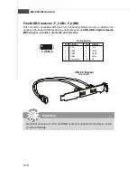
Page 34: ...ortant Note that the pins of VCC and GND must be connected correctly to avoid possible damage Front USBConnector F_USB1 F_USB2 This connector compliant with Intel I O Connectivity Design Guide is idea...

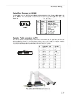
Page 35: ...PRND3 10 GND 11 PRND4 12 GND 13 PRND5 14 GND 15 PRND6 16 GND 17 PRND7 18 GND 19 ACK 20 GND 21 BUSY 22 GND 23 PE 24 GND 25 SLCT 26 GND 2 1 26 25 JLPT1 COM2 1 9 2 10 Serial Port Connector COM 2 This co...

Page 36: ...jumper to clear data Important You can clear CMOS by shorting 1 2 pin while the system is off Then return to 2 3 pin position Avoid clearing the CMOS while the system is on it will damage the mainboar...

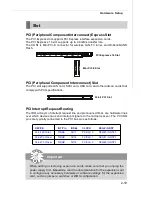
Page 37: ...t you unplug the power supply first Meanwhile read the documentation for the expansion card to configure any necessary hardware or software settings for the expansion card such as jumpers switches or...

Page 38: ...uses the same channel CF1 and IDE1 can support up to 2 IDE devices without CF device or 1 IDE device with 1 CF device If you install two IDE devices you must configure the second drive to Slave mode...

Page 39: ...IOS Setup program and allows you to configure the system for optimum use You may need to run the Setup program when An error message appears on the screen during the system booting up and requests you...

Page 40: ...HOENIX 2nd 5th digit refers to the model number 6th digit refers to the chipset as I Intel N nVidia and V VIA 7th 8th digit refers to the customer as MS all standard customers V1 0 refers to the BIOS...

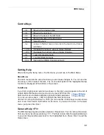
Page 41: ...hen you can use the control keys to enter values and move from field to field within a sub menu If you want to return to the main menu just press the Esc General Help F1 The BIOS setup program provide...

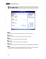
Page 42: ...atures Boot Use this menu to specify the priority of boot devices Security Use this menu to set supervisor and user passwords Chipset This menu controls the advanced features of the onboard Northbridg...

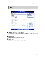
Page 43: ...n AMI BIOS Processor System Memory These items show the firmware and hardware specifications of your system Read only System Time The time format is Hour Minute Second System Date The date format is D...

Page 44: ...3 6 MS 9803 Mainboard Advanced CPU Configuration These items show the advanced specifications of your CPU Read only...

Page 45: ...3 7 BIOS Setup IDE Configuration ATA IDE Configuration This setting specifies the modes of the PATA SATA ports Configure SATA as s This setting specifies the function of the on chip SATA controller...

Page 46: ...in place of Cylinders Heads and Sectors Block Multi Sector Transfer Any selection except Disabled determines the number of sectors transferred per block PIO Mode Indicates the type of PIO Programmed...

Page 47: ...s setting specifies the I O port address and IRQ of the onboard parallel port Chassis Intrusion The field enables or disables the feature of recording the chassis intrusion status and issuing a warnin...

Page 48: ...VSB VBAT These items display the current status of all of the monitored hardware de vices components such as CPU voltage temperatures and all fans speeds CPUFAN0 CPUFAN1 Mode Setting These settings s...

Page 49: ...stem context is lost CPU or chipset and hard ware maintains all system context S3 STR The S3 sleep mode is a lower power state where the information of system configuration and open appli cations file...

Page 50: ...utton Resume On LAN This field specifies whether the system will be awakened from power saving modes when activity or input signal of onboard LAN is detected Resume On PME When setting to Enabled this...

Page 51: ...echnology is poised to eliminate many of the bottlenecks associated with HDD latency By enabling the majority of application workload to be written and read from a system cache instead of the HDD Robs...

Page 52: ...field allows you to select which MPS Multi Processor Specification ver sion to be used for the operating system You need to select the MPS version supported by your operating system To find out which...

Page 53: ...ed by the Trusted Computing Group TCG TPMs are special purpose integrated circuits ICs built into a variety of platforms to enable strong user authentication and machine attestation essential to preve...

Page 54: ...t or have any USB 1 1 2 0 driver installed such as DOS and SCO Unix USB 2 0 Controller Mode This setting specifies the operation mode of the onboard USB 2 0 controller Hotplug USB FDD Support Set to E...

Page 55: ...3 17 BIOS Setup Boot Boot Settings Configuration...

Page 56: ...ck This setting is to set the Num Lock status when the system is powered on Setting to On will turn on the Num Lock key when the system is powered on Setting to Off will allow users to use the arrow k...

Page 57: ...to gain access to their ROM setup utilities Boot Device Priority 1st Boot Device The items allow you to set the sequence of boot devices where BIOS attempts to load the disk operating system First pr...

Page 58: ...e This setting allows users to set the priority of the removable devices First press Enter to enter the sub menu Then you may use the arrow keys to select the desired device then press or PageUp PageD...

Page 59: ...upervisor Password controls access to the BIOS Setup utility These settings allow you to set or change the supervisor password User Password Change User Password User Password controls access to the s...

Page 60: ...3 22 MS 9803 Mainboard Chipset...

Page 61: ...at card Otherwise it defaults to the onboard graphics processor PEG Force X1 This BIOS feature allows you to convert a PCI Express X16 slot into a PCI Express X1 slot When Enabled the PCI Express X16...

Page 62: ...mum performance Setting it to DVMT Mode ensures that system memory is dy namically allocated for optimal balance between graphics and system performance DVMT FIXED Memory When set to DVMT FIXED Mode t...

Page 63: ...d SCO Unix GbE Controller This setting disables enables the onboard Gigabit Ethernet controller GbE LAN Boot When Enabled the BIOS attempts to boot from a LAN boot image before it attempts to boot fro...

Page 64: ...Setup Utility Discard Changes Abandon all changes and continue with the Setup Utility Load Optimal Defaults Use this menu to load the default values set by the mainboard manufacturer specifi cally fo...

Page 65: ...4 1 System Resources Chapter 4 System Resources This chapter provides information on the following system resources 1 Watch Dog Timer Setting p 4 2 2 AMI POST Code p 4 3 3 Resource List p 4 7...

Page 66: ...nds 1 Enter configuration mode mov dx SIO_IDX mov al 87h out dx al out dx al 2 Set to LDN 08 mov dx SIO_IDX mov al 07h out dx al mov dx SIO_DTA mov al 08h out dx al 3 Set WatchDog Timer mov dx SIO_IDX...

Page 67: ...4 3 System Resources AMI POST Code...

Page 68: ...MS 9803 Mainboard 4 4...

Page 69: ...4 5 System Resources...

Page 70: ...MS 9803 Mainboard 4 6...

Page 71: ...ADET0 AG10 22 I O SCLOCK 3 3v NC AH25 27 I O QRT_STATE0 3 3v EL_STATE0 AD16 28 I O QRT_STATE1 3 3v EL_STATE1 AG13 35 I O SATACLKREQ 3 3v CLK_SATA_OE AF9 38 I O SLOAD 3 3v NC AJ11 39 I O SDATAOUT0 3 3v...

Page 72: ...32 I O RSTOUT2 GP32 SCL VSB NC 91 31 I O GP31 VSB NC 92 30 I O GP30 VSB NC 67 57 O GP57 PSOUT VSB PWRBTN 68 56 I GP56 PSIN VSB IO_PWRBTN 64 37 I O GP37 VSB NC 72 53 I O GP53 PSON VSB PS_ON 73 52 I GP...

Page 73: ...B 80 45 O RTSB VSB RTSB 83 42 O SOUTB VSB SOUTB 78 47 I CTSB VSB CTSB 81 44 O DTRB VSB DTRB 85 40 I RIB VSB RIB 63 26 I O KBDAT VSB KBDAT 62 27 I O KBCLK VSB KBCLK 66 24 I O MSDAT VSB MSDAT 65 25 I O...

Page 74: ...0073 RTC and CMOS 0080 0090 DMA Controller Page Registers 0092 Port 92h 00A0 00A1 Interrupt Controller 2 00B2 00B3 APM Register 00C0 00DF DMA Controller 2 00F0 00FF Numeric Data Processor 01F0 01F7 Pr...

Page 75: ...A 00 UHCI USB Controller 8086 2835 00 1A 01 Unknown Device 8086 283A 00 1A 07 Unknown Device 8086 284B 00 1B 00 PCI to PCI Bridge 8086 283F 00 1C 00 UHCI USB Controller 8086 2830 00 1D 00 UHCI USB Con...

Page 76: ...ler IRQ2 Cascade Interrupt IRQ3 COM2 IRQ4 COM1 IRQ5 PCI Device IRQ6 PCI Device IRQ7 LPT1 IRQ8 RTC IRQ9 ACPI Controller Interrupt IRQ10 PCI Device IRQ11 PCI Device IRQ12 PS 2 Mouse IRQ13 Numeric Data P...

Reviews: