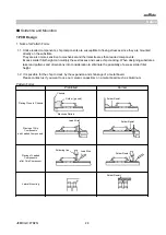
4-2.Flow Soldering
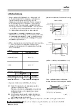
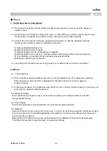
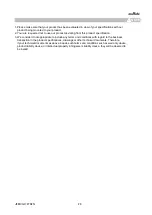
1. When sudden heat is applied to the components, the
[Standard Conditions for Flow Soldering]
mechanical strength of the components will decrease
because a sudden temperature change causes
deformation inside the components. In order to prevent
mechanical damage in the components, preheating should
be required for both of the components and the PCB board.
Preheating conditions are shown in table 2. It is required to
keep temperature differential between the solder and
the components surface (ΔT) as small as possible.
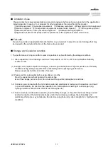
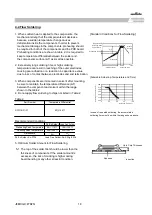
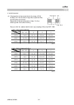
2. Excessively long soldering time or high soldering
temperature can result in leaching of the outer electrodes,
causing poor adhesion or a reduction in capacitance value
due to loss of contact between electrodes and end termination.
[Allowable Soldering Temperature and Time]
3. When components are immersed in solvent after mounting,
be sure to maintain the temperature difference (ΔT)
between the component and solvent within the range
shown in the table 2.
4. Do not apply flow soldering to chips not listed in Table 2.
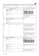
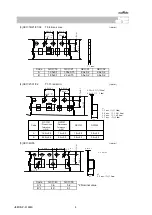
Table 2
In case of repeated soldering, the accumulated
soldering time must be within the range shown above.
Recommended Conditions
Pb-Sn Solder
Lead Free Solder
90
~
110
℃
100
~
120
℃
240
~
250
℃
250
~
260
℃
Air
N
2
Pb-Sn Solder: Sn-37Pb
Lead Free Solder: Sn-3.0Ag-0.5Cu
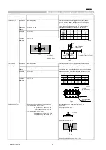
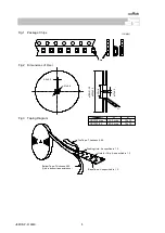
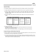
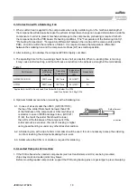
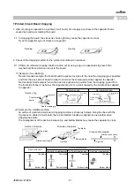
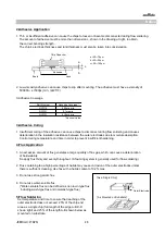
5. Optimum Solder Amount for Flow Soldering
5-1. The top of the solder fillet should be lower than the
thickness of components. If the solder amount is
excessive, the risk of cracking is higher during
board bending or any other stressful condition.
in section
Caution
Preheating Peak Temperature
Soldering Peak Temperature
Atmosphere
Part Number
GC
□
18/21/31
Temperature Differential
ΔT
≦
150
℃
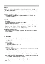
Up to Chip Thickness
Adhesive
!
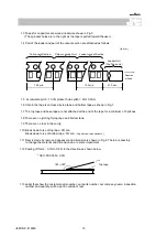
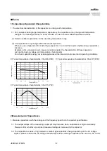
Temperature(℃)
Soldering Peak
Temperature
Preheating Peak
Soldering
Gradual
Cooling
Preheating
△T
30-90 seconds
5 seconds max.
Time
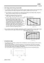
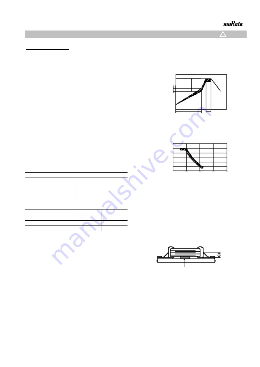
280
270
260
240
230
220
250
So
ld
er
ing
T
em
per
at
ur
e(
℃)
0
30
60
90
120
Soldering Time(sec.)
JEMCGC-2702N
18