background image

5.Washing

   Excessive ultrasonic oscillation during cleaning can cause the PCBs to resonate, resulting in cracked chips 
   or broken solder joints. Take note not to vibrate PCBs.

6.Electrical Test on Printed Circuit Board

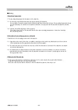
1. Confirm position of the backup pin or specific jig, when inspecting the electrical performance of a 
    capacitor after mounting on the printed circuit board.

    1-1. Avoid bending the printed circuit board by the pressure of a test-probe, etc.
          The thrusting force of the test probe can flex the PCB, resulting in cracked chips or open solder
          joints. Provide backup pins on the back side of the PCB to prevent warping or flexing.
          Install backup pins as close to the test-probe as possible.

    1-2. Avoid vibration of the board by shock when a test -probe contacts a printed circuit board.

[Not Recommended]

[Recommended]

7.Printed Circuit Board Cropping

1. After mounting a capacitor on a printed circuit board, do not apply any stress to the capacitor that
    caused bending or twisting the board.

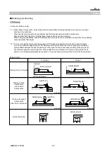
    1-1. In cropping the board, the stress as shown at right may cause the capacitor to crack.
           Cracked capacitors may cause deterioration of the insulation resistance, and result in a short.
           Avoid this type of stress to a capacitor. 

 [Bending]

 [Twisting]

2. Check the cropping method for the  printed circuit board in advance.

    2-1. Printed circuit board cropping shall be carried out by using a jig or an apparatus (Disk separator, router 
           type separator, etc.) to prevent the mechanical stress that can occur to the board.

* When a board separation jig or disk separator is used, if the following precautions are not observed, 
   a large board deflection stress will occur and the capacitors may crack. 
   Use router type separator if at all possible.

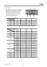
Caution

Notes

Hand and nipper
separation apply a high
level of stress.
Use another method.

· Board handling
· Board bending direction
· Layout of capacitors

· Board handling
· Layout of slits
· Design of V groove
· Arrangement of blades
· Controlling blade life

Board handling

Recommended

High

Medium

Medium

Low

Level of stress on board 

×

*

*

Board Separation Method

Hand Separation

Nipper Separation

(1) Board Separation Jig

Board Separation Apparatus

2) Disk Separator

3) Router Type Separator

Peeling


Test-probe


Backup 
Pin


Test-probe


① 

1A 


JEMCGC-2701W

20

Summary of Contents for GRM0225C1E8R4BDAE

Page 1: ...p Range Ref Temp 8 Packaging 6 Capacitance Tolerance 8 4 pF Temp coeff or Cap Change 0 1 pF This product specification is applied to Chip Monolithic Ceramic Capacitor used for General Electronic equipment 2 T 0 2 0 02 55 to 125 C 0 30 ppm C 25 to 125 C 25 C 4 Rated Voltage Specifications and Test Methods Operating Temp Range L f180mm Reel EMBOSSED W4P1 40000 pcs Reel 3 Temperature Characteristics ...

Page 2: ...125max W V 6 3V 0 15max 9 Capacitance No bias Within the specified R6 Within 15 The capacitance change should be measured after 5min at each Temperature tolerance Table A 1 55 C to 85 C specified temp stage Characteristics R7 Within 15 55 C to 125 C 1 Temperature Compensating Type C8 Within 22 The capacitance drift is calculated by dividing the differences between 55 C to 105 C the maximum and min...

Page 3: ...u solder solution at 270 5 for 10 0 5 seconds Q D F 30pF and over Q 1000 R6 R7 C8 L8 Set at room temperature for 24 2 hours then measure 30pF and beloow Q 400 20C W V 100V 0 025max C 0 068mF Initial measurement for high dielectric constant type 0 05max C 0 068mF Perform a heat treatment at 150 0 10 C for one hour and then set C Nominal Capacitance pF W V 50V 25V 0 025max at room temperature for 24...

Page 4: ...asurement W V 16V 10V 0 05max W V 6 3V 4V 0 075max C 3 3mF 0 125max C 3 3mF R9 W V 50V 0 075max E4 W V 25V 0 05max F5 W V 25Vmin 0 075max C 0 1mF 0 125max C 0 1mF W V 16V 10V 0 15max W V 6 3V 0 2max I R More than 500MΩ or 25Ω F Whichever is smaller 18 High Temperature The measured and observed characteristics should satisfy Solder the capacitor on the test jig glass epoxy board shown in Fig 3 Load...

Page 5: ...s fabric base epoxy resin Thickness 1 6mm GRM02 GRM03 GRM15 t 0 8mm Thickness 1 6mm GRM02 GRM03 GRM15 t 0 8mm Copper foil thickness 0 035mm Copper foil thickness 0 035mm Gray colored part of Fig 1 Solder resist Coat with heat resistant resin for solder Fig 1 in mm Fig 3 in mm Fig 2 in mm SPECIFICATIONS AND TEST METHODS Type Dimension mm a b c GRM02 0 2 0 56 0 23 GRM03 0 3 0 9 0 3 GRM15 0 4 1 5 0 5...

Page 6: ...0 10000 6 4000 10000 9 4000 3000 10000 10000 A B 3000 10000 6 9 4000 10000 M X 3000 10000 C 2000 6000 9 4000 10000 A M 3000 10000 N 2000 8000 C 2000 6000 R D E 1000 4000 M 1000 5000 N R D 1000 4000 E 500 2000 S 500 1500 M 1000 5000 N C R D 1000 4000 E 500 F 300 1500 1 2 Dimensions of Tape 1 GR 01 02 W4P1 CODE L in mm Package GRM F Type Type GR 21 GR 31 GR 32 GR 43 Paper Tape GR 55 GR 15 1 2 1 0 0 ...

Page 7: ...0 0 05 4 0 0 1 φ1 5 0 1 0 1 75 0 1 8 0 0 3 3 5 0 05 A B t 1 0 0 05 Type LW Dimensions Tolerance Chip A 3 B 3 t GR 03 0 03 0 37 0 67 0 5 max 0 05 0 39 0 69 GR 15 0 05 0 65 1 15 0 8 max 0 1 0 70 1 20 0 15 0 72 1 25 0 2 0 75 1 35 3 Nominal value Type LW Dimensions Tolerance Chip A B t GRM033 0 03 0 05 0 37 0 67 0 5max GRM155 0 05 0 65 1 15 0 8max Nominal value JEMCGP 01796C 7 ...

Page 8: ... 15 2 30 0 15 1 15 max 9 0 2 max 0 85 0 05 0 85 0 1 0 85 0 15 0 1 0 85 0 0 2 0 2 0 85 0 15 0 05 1 50 0 20 2 30 0 20 1 7 max Plastic Tape A 0 1 1 0 0 0 2 1 45 0 20 2 25 0 20 0 2 1 0 0 2 1 50 0 20 2 30 0 20 B 0 1 1 25 0 1 1 45 0 20 2 25 0 20 0 15 1 25 0 15 1 50 0 20 2 30 0 20 2 0 max 0 2 1 25 0 2 GR 31 6 0 15 0 6 0 1 2 00 0 20 3 60 0 20 1 15 max Paper Tape 9 0 2 max 0 85 0 1 M 0 15 1 15 0 1 1 90 0 2...

Page 9: ...M F Type φ1 5 0 1 0 4 0 0 1 8 0 0 1 φ1 5 0 2 0 12 0 0 3 5 5 0 1 1 75 0 1 A 1 2 5 max T 1 8mm 3 7 max T 2 0 2 5mm 4 7 max 2 8 T 3 2mm B 1 2 0 0 1 0 3 0 1 Type A 2 B 2 GR 43 3 60 4 90 GR 55 5 20 6 10 2 Nominal value JEMCGP 01796C 9 ...

Page 10: ...pecified in 1 2 Base Tape As specified in 1 2 Bottom Tape Thickness 0 05 Only a bottom tape existence W w1 GR 01 02 8 0 max 5 1 5 GR 32 max 16 5 max 10 1 5 GR 43 55 20 5 max 14 1 5 φ180 0 3 0 φ330 2 0 φ50 min φ13 0 5 2 0 0 5 Chip in mm Fig 1 Package Chips Fig 2 Dimensions of Reel Fig 3 Taping Diagram JEMCGP 01796C 10 ...

Page 11: ...There are no fuzz in the cavity 1 10 Break down force of top tape 5N min Break down force of bottom tape 5N min Only a bottom tape existence 1 11 Reel is made by resin and appeaser and dimension is shown in Fig 2 There are possibly to change the material and dimension due to some impairment 1 12 Peeling off force 0 1N to 0 6N in the direction as shown below GR 01 02 03 0 05N 0 5N 1 13 Label that s...

Page 12: ...t with the termination external electrodes or lead wires of capacitors and result in poor solderability Do not store the capacitors in an atmosphere consisting of corrosive gas e g hydrogen sulfide sulfur dioxide chlorine ammonia gas etc 1 3 Due to moisture condensation caused by rapid humidity changes or the photochemical change caused by direct sunlight on the terminal electrodes and or the resi...

Page 13: ...trical short circuit caused by the breakdown of the internal dielectric layers The time duration until breakdown depends on the applied voltage and the ambient temperature 4 Type of Applied Voltage and Self heating Temperature 1 Confirm the operating conditions to make sure that nolarge current is flowing into the capacitor due to the continuous application of an AC voltage or pulse voltage When a...

Page 14: ...ch the capacitance value decreases with the passage of time When you use a high dielectric constant type capacitors in a circuit that needs a tight narrow capacitance tolerance e g a time constant circuit please carefully consider the characteristics of these capacitors such as their aging voltage and temperature characteristics In addition check capacitors using your actual appliances at the inte...

Page 15: ...ion surface A C Mounting Capacitors Near Screw Holes When a capacitor is mounted near a screw hole it may be affected by the board deflection that occurs during the tightening of the screw Mount the capacitor in a position as far away from the screw holes as possible 2 Information before Mounting 1 Do not re use capacitors that were removed from the equipment 2 Confirm capacitance characteristics ...

Page 16: ...e so as not to bend the printed circuit board 2 Adjust the nozzle pressure within a static load of 1N to 3N during mounting Incorrect Correct 2 Dirt particles and dust accumulated between the suction nozzle and the cylinder inner wall prevent the nozzle from moving smoothly This imposes greater force upon the chip during mounting causing cracked chips Also the locating claw when worn out imposes u...

Page 17: ...table 1 Table 1 GRM01 02 03 15 18 21 31 GRM32 43 55 In the case of repeated soldering the accumulated Recommended Conditions soldering time must be within the range shown above Lead Free Solder Sn 3 0Ag 0 5Cu 4 Optimum Solder Amount for Reflow Soldering 4 1 Overly thick application of solder paste results in a excessive solder fillet height This makes the chip more susceptible to mechanical and th...

Page 18: ... and end termination 4 When components are immersed in solvent after mounting be sure to maintain the temperature differential ΔT between the component and solvent within the range shown in the table 2 In the case of repeated soldering the accumulated soldering time must be within the range shown above Recommended Conditions Lead Free Solder Sn 3 0Ag 0 5Cu 5 Optimum Solder Amount for Flow Solderin...

Page 19: ...mponent 2 1 If the distance from the hot air outlet of the spot heater to the component is too close cracks may occur due to thermal shock To prevent this problem follow the conditions shown in Table 4 2 2 In order to create an appropriate solder fillet shape it is recommended that hot air be applied at the angle shown in Figure 1 Table 4 Distance 5mm or more Hot Air Application angle 45 Figure 1 ...

Page 20: ... stress as shown at right may cause the capacitor to crack Cracked capacitors may cause deterioration of the insulation resistance and result in a short Avoid this type of stress to a capacitor Bending Twisting 2 Check the cropping method for the printed circuit board in advance 2 1 Printed circuit board cropping shall be carried out by using a jig or an apparatus Disk separator router type separa...

Page 21: ...eparation point 2 Example of a Disk Separator An outline of a disk separator is shown as follows As shown in the Principle of Operation the top blade and bottom blade are aligned with the V grooves on the printed circuit board to separate the board In the following case board deflection stress will be applied and cause cracks in the capacitors 1 When the adjustment of the top and bottom blades are...

Page 22: ...ard Periodically check and adjust the bottom dead point 2 2 Inserting Components with Leads into Boards When inserting components transformers IC etc into boards bending the board may cause cracks in the capacitors or cracks in the solder Pay attention to the following Increase the size of the holes to insert the leads to reduce the stress on the board during insertion Fix the board with backup pi...

Page 23: ...t is not turned off or unplugged the hazards may be worsened by supplying continuous power 2 In this type of situation do not allow face and hands to come in contact with the capacitor or burns may be caused by the capacitor s high temperature 2 2 Disposal of waste When capacitors are disposed of they must be burned or buried by an industrial waste vendor with the appropriate licenses 2 3 Circuit ...

Page 24: ...nt of capacitors 1 1 Capacitors when used in the above unsuitable operating environments may deteriorate due to the corrosion of the terminations and the penetration of moisture into the capacitor 1 2 The same phenomenon as the above may occur when the electrodes or terminals of the capacitor are subject to moisture condensation 1 3 The deterioration of characteristics and insulation resistance du...

Page 25: ...ip is different depending on PCB material and structure When the thermal expansion coefficient greatly differs between the board used for mounting and the chip it will cause cracking of the chip due to the thermal expansion and contraction When capacitors are mounted on a fluorine resin printed circuit board or on a single layered glass epoxy board it may also cause cracking of the chip for the sa...

Page 26: ... within 0 20 3 2 1 6 0 30 in mm GRM01 0 25 0 125 0 10 to 0 11 0 07 to 0 12 0 125 to 0 145 0 4 to 0 6 0 40 to 0 50 GRM31 3 2 1 6 2 2 to 2 6 1 0 to 1 1 GRM02 0 4 0 2 0 16 to 0 2 0 12 to 0 18 Notice L W a b c 0 8 to 0 9 GRM18 0 6 to 0 8 1 6 0 8 0 6 to 1 0 c 2 0 1 25 1 0 to 1 2 GRM21 a L W Dimensions Tolerance 0 9 to 1 0 0 8 to 1 1 1 0 to 1 4 b 0 2 to 0 23 GRM03 0 6 0 3 0 2 to 0 3 0 6 1 25 GRM21 0 6 t...

Page 27: ...throughout A foaming system is generally used for flow solderring 2 Flux containing too high a percentage of halide may cause corrosion of the outer electrodes unless there is sufficient cleaning Use flux with a halide content of 0 1 max 3 Do not use strong acidic flux 4 Do not use water soluble flux Water soluble flux can be defined as non rosin type flux including wash type flux and non wash typ...

Page 28: ... performance of a capacitor may be affected by the conditions during transportation 1 1 The capacitors shall be protected against excessive temperature humidity and mechanical force during transportation 1 Climatic condition low air temperature 40 change of temperature air air 25 25 low air pressure 30 kPa change of air pressure 6 kPa min 2 Mechanical condition Transportation shall be done in such...

Page 29: ...ication 3 We consider it not appropriate to include any terms and conditions with regard to the business transaction in the product specifications drawings or other technical documents Therefore if your technical documents as above include such terms and conditions such as warranty clause product liability clause or intellectual property infringement liability clause they will be deemed to be inva...

Reviews: