■
Soldering and Mounting
1.PCB Design
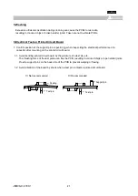
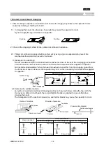
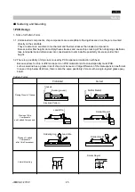
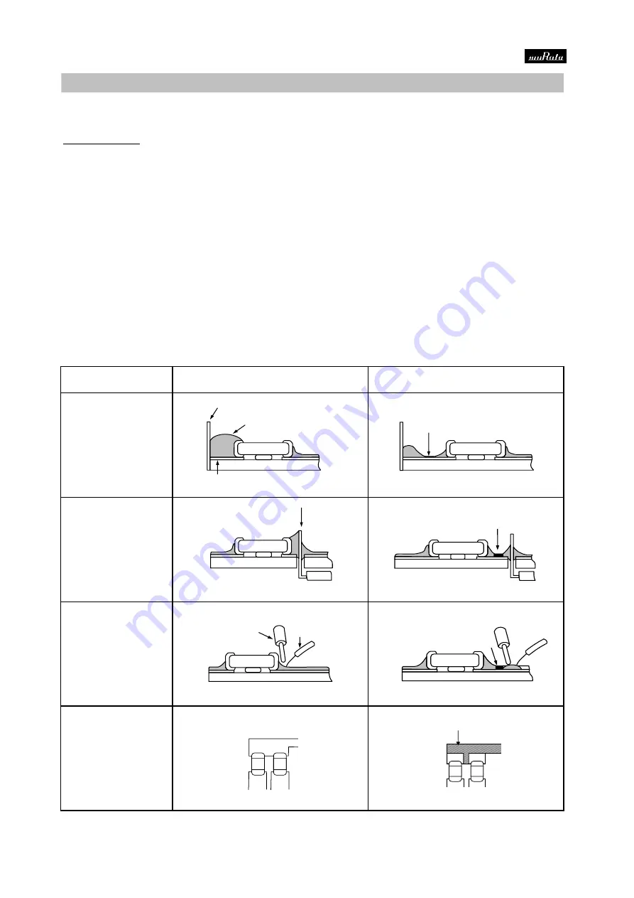
1. Notice for Pattern Forms
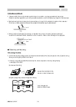
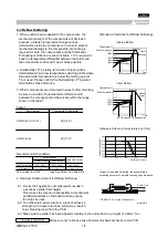
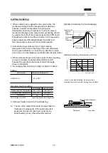
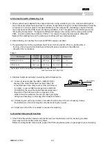
1-1. Unlike leaded components, chip components are susceptible to flexing stresses since they are mounted
directly on the substrate.
They are also more sensitive to mechanical and thermal stresses than leaded components.
Excess solder fillet height can multiply these stresses and cause chip cracking. When designing substrates,
take land patterns and dimensions into consideration to eliminate the possibility of excess solder fillet
height.
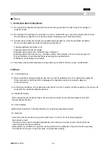
1-2.There is a possibility of chip crack caused by PCB expansion/contraction with heat.
Because stress for chip is different depend on PCB material and structure.Especially metal PCB
such as alumina has a greater risk of chip crack because of large difference of thermal expansion coefficient.
In case of chip below 0402 size, there is also the same possibility of crack with a single-layered glass epoxy
board.
Pattern Forms
Placing of Leaded
Components
after Chip Component
Lateral Mounting
Notice
Prohibited
Correct
Placing Close to Chassis
Placing of Chip
Components
and Leaded Components
Chassis
Solder (ground)
Electrode Pattern
Solder Resist
Lead Wire
Solder Resist
Lead Wire
Soldering Iron
Solder Resist
ソルダレジスト
Solder Resist
JEMCGC-2701V
25

