Application Note
[Page 9]
Design Considerations of EMW3239
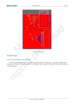
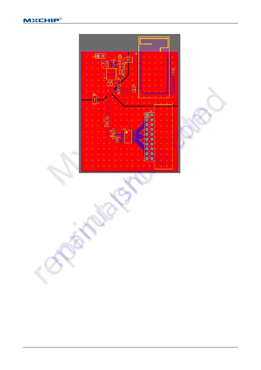
Figure 2.4 PCB Design
RF Design
2.5
2.5.1
On-board PCB Antenna Design
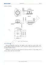
The main board PCB should be over 16mm far away from other metal components. Copper, route, closing to metal
element is not allowed if the structure needed. P1 to P8 should connect to ground with copper. PCB part below antenna
could be hollowed up.

