background image

Application  Note 


[Page  16] 

Design Considerations of EMW3239


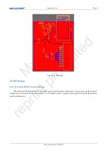
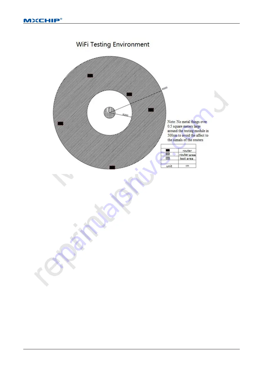
Figure 3.9 Position of Routers 


Important Statement 

3.8

MXCHIP has a duty to make sure there is no quality problem when sell the module to customers.   

Customers have the rights to ask MXCHIP to exchange goods if the product has quality problem. 

If  the  customer  find  the  problem  after  welding  the  module  on  board  without  testing  at  the  beginning, 

MXCHIP is only responsible for the compensation of the module part. 

MXCHIP would help customers solve technical problem in developing firmware without save any MVA/bin 

file.  Customers  should  save  different  development  vision  and  download  relative  vision  in  module  before 

producing. 

Summary of Contents for EMW3239

Page 1: ...rapid mass production Users should be familiar with the document to pre consider and avoid problems effectively in designing producing programming and testing More Help For more products information p...

Page 2: ...tails 2016 9 23 0 1 Initial document 2016 9 29 0 2 Add reference circuit Add description of pin function and design consideration Add position figure of PCB 2016 12 2 0 3 Add Module downloading method...

Page 3: ...ADING MODE 12 3 2 SYSTEM CONNECTION 13 3 3 SERIAL PORT SELECTION 13 3 4 J FLASH 13 3 5 J FLASH SET UP 14 3 6 TESTING 15 3 7 3 7 1 Environment Set Up 15 IMPORTANT STATEMENT 16 3 8 4 SMT 17 STENCILS 17...

Page 4: ...ch Set Up 13 Figure 3 2Power Light 13 Figure 3 3 Name in Device Manager 13 Figure 3 4 Install J Flash 14 Figure 3 5 J Flash signature 14 Figure 3 6 Target Interface Set Up 14 Figure 3 7 MCU Set Up 15...

Page 5: ...in designing producing programming and testing Suitable module type EMW3239 Phase of attention Hardware design Firmware testing SMT Online update Basic Characteristics Each module has a unique MAC ad...

Page 6: ...Technology Co Ltd EMW3239 E IPEX brass pipe Antenna Optional Dongguan Aosiya Antenna Technology Co Ltd Antenna Parameter Parameter EMW3239 E EMW3239 P Antenna Type Brass pipe Antenna PCB Antenna Freq...

Page 7: ...d in EMW3239 as shown in figure 3 to simplify debugging and disassembling for developers as well as offering varied selection Also it is benefit for SMT patch and hand welding Solder mask openness has...

Page 8: ...n 1 2 1 EMW3239 Pin Definition Pins Name Type I O Level Multi select Function User 1 NC 2 PB2 I O FT GPIO BOOT1 3 NC 4 PB15 I O FT SPI2_MOSI GPIO TIM12_CH2 I2S2_SD 5 PB12 I O FT SPI2_NSS GPIO CAN2_RX...

Page 9: ...CH1 I2S2_MCK DEBUG_OUT Unusable 9 PA15 I O FT GPIO JTDI TIM2_CH1 USART1_TXD EasyLink 10 VBAT S VBAT 11 NC 12 PC7 I O FT UART6_RXD GPIO TIM3_CH2 I2S2_CK DEBUG_IN Unusable 13 NRST I O FT RESET 14 PC0 I...

Page 10: ...T1_RXD GPIO TIM4_CH2 I2C1_SDA USER_UART_RX 30 PB6 I O FT UART1_TXD GPIO TIM4_CH1 I2C1_SCL USER_UART_TX 31 PB4 I O FT GPIO JTRST TIM3_CH1 32 NC 33 PA10 I O FT USB_ID GPIO TIM1_CH3 34 PA5 I O TC GPIO AD...

Page 11: ...for users 4 S stands for power supply I stands for input pins and I O stands for input and output pins 5 FT 5V tolerant The maximum voltage should be less than VCC when set as analog input output or c...

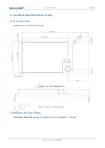
Page 12: ...ations in Hardware Design Mechanical Size 2 1 Mechanical size of EMW3031 Unit mm Figure 2 1 Top View of Mechanical Size Figure 2 2 Side View of Mechanical Size Reference Package Design 2 2 Solder mask...

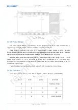
Page 13: ...e Details about the requirements should refer to the datasheet of DC DC device Maximum output current and dissipate heat should be aware for the using of LDO voltage drop is 1 7V when voltage reduce f...

Page 14: ...trol UART communications and one normal UART communication Pin 29 and Pin 30 are used as serial port of users Test information download and communication Pin 8 and Pin 12 is debugging ports running lo...

Page 15: ...ign 2 5 2 5 1 On board PCB Antenna Design The main board PCB should be over 16mm far away from other metal components Copper route closing to metal element is not allowed if the structure needed P1 to...

Page 16: ...n order to reduce the influence from metal components to PCB antenna and wireless signal it is better to mount EMW3239 on four parts Figure 2 6 Position of the Module 2 5 2 External Antenna Size of ex...

Page 17: ...ule Human body model HBM is 2000V charged device model CDM is 500V Position of ESD protected components should be reserved if the products require higher ESD requirement such as pins connect to USB an...

Page 18: ...3 2Download Websites Name Function Websites FWUpdate Download http pan baidu com s 1kVEwnNh MicoQcAutoCheck4 0 Test http pan baidu com s 1kVEwnNh CP210x_VCP_Windows USB Drever http www silabs com pro...

Page 19: ...ager after installing System Connection 3 3 Module connects to develop board of EMW3031 with USB Green light D1 on the develop board enable when connecting Figure 3 2Power Light Serial Port Selection...

Page 20: ...J Flash JFlash V6 00 would be found after installing Figure 3 5 J Flash signature J Flash Set Up 3 6 Use ALT F7 or open Options then click project settings Select SWD in Target Interface ST STM32F412...

Page 21: ...3 7 MCU Set Up Figure 3 8 Production Set Up Click OK after set up There would be no more set up in following downloading if save the set up Testing 3 7 3 7 1 Environment Set Up Turn on 5 routers that...

Page 22: ...MXCHIP to exchange goods if the product has quality problem If the customer find the problem after welding the module on board without testing at the beginning MXCHIP is only responsible for the compe...

Page 23: ...extend 0 15mm in order to improving solder wicking If there is no AOI testing check module by eye is available to reduce the Pseudo Soldering Figure 4 1 Stencils size Temperature Curve of Secondary Re...

Page 24: ...tself and return the results from serial port by sending testing command through serial port 5 1 2 Complete Secondary Development of Firmware Application of customer is based on secondary development...

Page 25: ...sultation or purchase the product please contact Mxchip during working hours From Monday to Friday morning 9 00 12 00 afternoon 13 00 18 00 Telephone 86 21 52655026 Contact address 9th Floor No 5 Lane...

Page 26: ...or more of the following measures Reorient or relocate the receiving antenna Increase the separation between the equipment and receiver Connect the equipment into an outlet on a circuit different from...

Reviews: