Chapter 3
Analog Output Timing/Control
©
National Instruments Corporation
3-109
DAQ-STC Technical Reference Manual
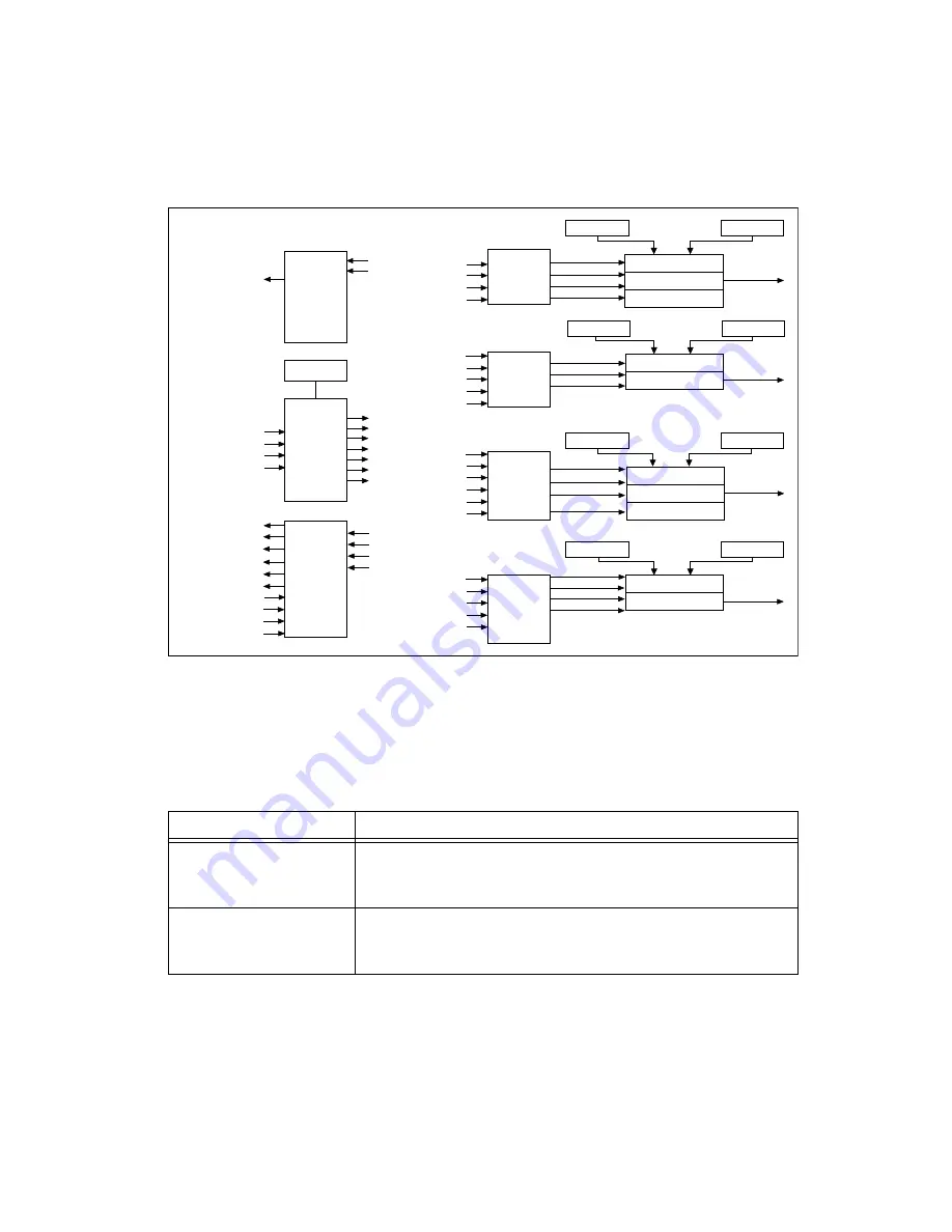
Figure 3-34.
AOTM Block Diagram
3.8.1 Internal Signals and Operation
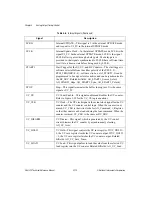
Table 3-6 contains brief descriptions of the internal signals shown in the block diagram
or discussed in section
.
Table 3-6.
Internal Signals
Signal
Description
AO_END1
End on UC_TC—This signal is the schematic name for the
synchronized version of the register map bitfield
AO_End_On_UC_TC.
AO_END2
End on BC_TC—This signal is the schematic name for the
synchronized version of the register map bitfield
AO_End_On_BC_TC.
AO_IN_TIMEBASE1
IN_TIMEBASE2
PFI<0..9>
AOFREQ
CPUDACWR
AO_ADDR<0..3>
UPDATE
UPDATE2
AOFEF
AOFHF
START1
STOP
UI2_SRC
UI_SRC
BC_SRC
EXT_GATE
EXT_GATE2
RTSI_TRIGGER<0..6>
START1
STOP
BC_TC
BC_SRC
UC_TC
EXT_GATE
START1
EXT_GATE
UI_SRC
BC_TC
UI_TC
START1
STOP
BC_TC
BC_SRC
START1
STOP
UI2_SRC
UI2_TC
EXT_GATE2
START1
STOP
BC
Control
Logic
UI
Control
Logic
UC
Control
Logic
UI2
Control
Logic
Output
Control
Routing
Logic
Interrupt
Control
Trg/Src SEL
UI2 Load A
UI2 Load B
UC Load A
UC Load B
BC Load A
BC Load B
MUX
BC Counter
BC Save
MUX
UC Counter
UC Save
MUX
UI2 Counter
UI2_CLK
UI2_LOAD
UI2_CE
UI2_LOAD_SRC
UC_HOLD
UC_CLK
UC_CE
UC_LOAD_SRC
UI_CLK
UI_CE
UI_LOAD_SRC
BC_LOAD_SRC
BC_HOLD
BC_CLK
BC_CE
BC_TC
UI_TC
UC_TC
UI2_TC
IRQ_OUT<0..7>
TMRDACWR
AOFFF
CPUDACREQ
UI_SRC
UI_TC
UI2_SRC
UI2_TC
MUX
UI Counter
UI Load A
UI Load B

