Chapter 3
Analog Output Timing/Control
DAQ-STC Technical Reference Manual
3-108
©
National Instruments Corporation
3.7.12.2 UC_TC
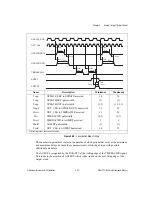
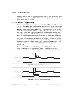
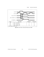
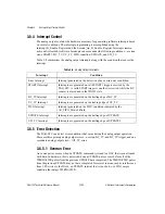
Figure 3-33 shows the delays associated with the UC_TC signal.
Figure 3-33.
UC_TC Delay
3.8 Detailed Description
This section describes the AOTM module in detail. You need not read this section unless you
need to understand the inner workings of the circuit. This section refers to bitfields in the
AOTM related registers in the DAQ-STC register map. See Appendix B,
, for more information on the register addresses containing these bitfields.
Figure 3-34 shows a block diagram of the AOTM. The AOTM contains four special purpose
counters—the BC, UI, UI2, and UC counters. Each counter has dual-load registers (A and B)
to handle two parameters for each timing layer. In addition to the counters, the primary logic
blocks are the counter control blocks, the trigger block, the interrupt control block, and the
output control block.
Name
Description
Minimum
Maximum
Tuc
UC Source to UC_TC
13
75
All timing values are in nanoseconds.
UC Source
UC_TC
Tuc
Tuc

