background image

11-4

|

ni.com

Chapter 11

Triggering

Routing Analog Comparison Event to an Output 
Terminal

You can route Analog Comparison Event out to any PFI <0..15> or RTSI <0..7> terminal.

Analog Trigger Types

Configure the analog trigger circuitry to different triggering modes:

Analog Edge Triggering

—Configure the analog trigger circuitry to detect when the 

analog signal is below or above a level you specify.

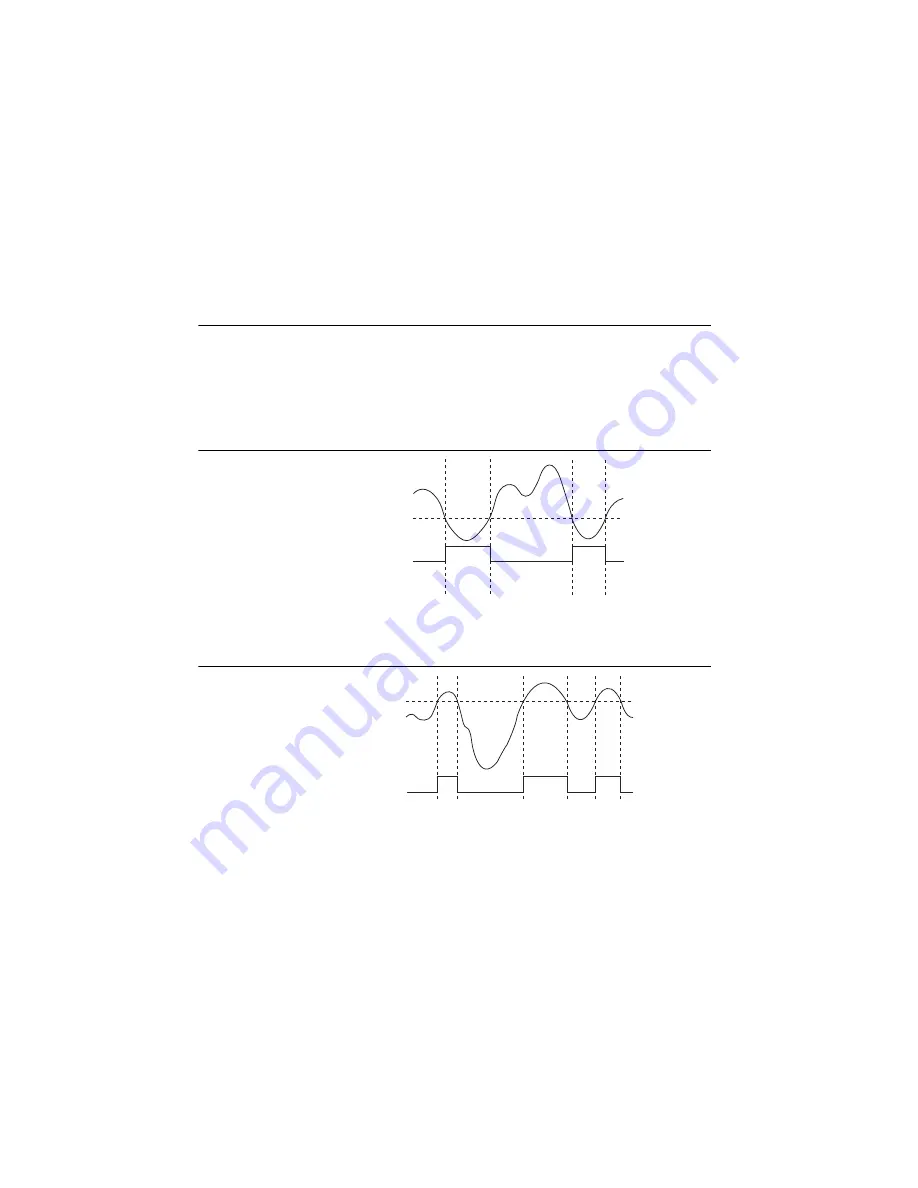
In below-level analog triggering mode, shown in Figure 11-4, the trigger is generated when 
the signal value is less than Level.

Figure 11-4.  

Below-Level Analog Triggering Mode

In above-level analog triggering mode, shown in Figure 11-5, the trigger is generated when 
the signal value is greater than Level.

Figure 11-5.  

Above-Level Analog Triggering Mode

Analog Edge Triggering with Hysteresis

—Hysteresis adds a programmable voltage 

region above or below the trigger level that an input signal must pass through before the 
DAQ device recognizes a trigger condition, and is often used to reduce false triggering due 
to noise or jitter in the signal.

Analog Edge Trigger with Hysteresis (Rising Slope)—When using hysteresis with a 
rising slope, you specify a trigger level and amount of hysteresis. The high threshold 
is the trigger level; the low threshold is the trigger level minus the hysteresis.

Level

An

a

log Comp

a

ri

s

on Event

Level

An

a

log Comp

a

ri

s

on Event

Summary of Contents for DAQ X NI 634 Series

Page 1: ...PXIe 6349...

Page 2: ...DAQ X Series X Series User Manual NI 632x 634x 635x 636x 637x 638x 639x Devices X Series User Manual ni com manuals Deutsch Fran ais May 2019 370784K 01...

Page 3: ...phone numbers email addresses and current events National Instruments Corporate Headquarters 11500 North Mopac Expressway Austin Texas 78759 3504 USA Tel 512 683 0100 For further support information...

Page 4: ...ESS FOR A PARTICULAR PURPOSE TITLE OR NON INFRINGEMENT AND ANY WARRANTIES THAT MAY ARISE FROM USAGE OF TRADE OR COURSE OF DEALING NI DOES NOT WARRANT GUARANTEE OR MAKE ANY REPRESENTATIONS REGARDING TH...

Page 5: ...es independent from National Instruments and have no agency partnership or joint venture relationship with National Instruments Patents For patents covering National Instruments products technology re...

Page 6: ...unting 1 8 USB Device LEDs 1 9 USB Cable Strain Relief 1 9 USB Device Security Cable Slot 1 10 Device Pinouts 1 10 Device Specifications 1 10 Device Accessories and Cables 1 10 Chapter 2 DAQ System Ov...

Page 7: ...4 Configuring AI Ground Reference Settings in Software 4 6 Multichannel Scanning Considerations 4 6 Analog Input Data Acquisition Methods 4 9 Software Timed Acquisitions 4 9 Hardware Timed Acquisitio...

Page 8: ...al 4 30 AI Hold Complete Event Signal 4 30 AI Start Trigger Signal 4 30 AI Reference Trigger Signal 4 32 AI Pause Trigger Signal 4 34 Getting Started with AI Applications in Software 4 35 Analog Input...

Page 9: ...AO Pause Trigger Signal to an Output Terminal 5 8 AO Sample Clock Signal 5 8 Using an Internal Source 5 8 Using an External Source 5 9 Routing AO Sample Clock Signal to an Output Terminal 5 9 Other T...

Page 10: ...tion 6 13 DO Sample Clock Signal 6 13 Using an Internal Source 6 13 Using an External Source 6 14 Routing DO Sample Clock to an Output Terminal 6 14 Other Timing Requirements 6 14 DO Sample Clock Time...

Page 11: ...urement 7 11 Frequency Measurement 7 11 Low Frequency with One Counter 7 12 High Frequency with Two Counters 7 12 Large Range of Frequencies with Two Counters 7 13 Sample Clocked Buffered Frequency Me...

Page 12: ...e 7 38 Routing Counter n Gate to an Output Terminal 7 38 Counter n Aux Signal 7 38 Routing a Signal to Counter n Aux 7 38 Counter n A Counter n B and Counter n Z Signals 7 39 Routing Signals to A B an...

Page 13: ...2 10 MHz Reference Clock 9 3 Synchronizing Multiple Devices 9 3 PXI Express Devices 9 3 PCI Express Devices 9 3 USB Devices 9 4 Real Time System Integration RTSI 9 4 RTSI Connector Pinout 9 5 Using R...

Page 14: ...arison Event to an Output Terminal 11 4 Analog Trigger Types 11 4 Analog Trigger Accuracy 11 6 Appendix A Device Specific Information Appendix B Where to Go from Here Appendix C Troubleshooting Append...

Page 15: ...out A 28 Figure A 20 NI USB 6353 6363 Screw Terminal Pinout A 30 Figure A 21 NI USB 6363 Pinout A 31 Figure A 22 NI PXIe PXIe 6356 6366 6386 6396 and PCIe PXIe 6376 Pinout A 33 Figure A 23 NI USB 6366...

Page 16: ...or digital ground or to any other voltage source on the X series device or any other device Doing so can damage the device and the computer NI is not liable for damage resulting from such a connectio...

Page 17: ...latory rules Notice To ensure the specified EMC performance product installation requires either special considerations or user installed add on devices Refer to the product installation instructions...

Page 18: ...s and cables Unpacking The X Series device ships in an antistatic package to prevent electrostatic discharge ESD ESD can damage several components on the device Caution Never touch the exposed pins of...

Page 19: ...s caused by short term fluctuations in the environment You can initiate self calibration using Measurement Automation Explorer MAX by completing the following steps Note Disconnect all external signal...

Page 20: ...arth ground connections refer to the document Grounding for Test and Measurement Devices by going to ni com info and entering the Info Code emcground You can attach and solder a wire to the chassis gr...

Page 21: ...2 Ensure that the ferrite bead is as close to the end of the power cable as practical Install the snap on ferrite bead by opening the housing and looping the power cable once through the center of th...

Page 22: ...using the USB X Series mounting kit part number 781514 01 not included in your USB X Series device kit Refer to Figure 1 3 1 Use three 8 32 flathead screws to attach the backpanel wall mount to the pa...

Page 23: ...d in the kit as shown in Figure 1 4 Tighten the screws to a torque of 0 4 N m 3 6 lb in Figure 1 4 Attaching the DIN Rail Clip to the Backpanel Wall Mount 2 Clip the bracket onto the DIN rail as shown...

Page 24: ...device READY and ACTIVE LEDs USB Cable Strain Relief NI USB 63xx Devices You can provide strain relief for the USB cable by using the jackscrew on the locking USB cable included in the USB X Series d...

Page 25: ...on that accompanied the security cable Note The security cable slot on the USB device might not be compatible with all laptop lock cables Device Pinouts Refer to Appendix A Device Specific Information...

Page 26: ...les that connect the various devices to the accessories the X Series device programming software and PC The following sections cover the components of a typical DAQ system Figure 2 1 Components of a T...

Page 27: ...ggering modes Independent AI AO DI DO and counter FIFOs Generation and routing of RTSI signals for multi device synchronization Generation and routing of internal and external timing signals Four flex...

Page 28: ...compliance with Electromagnetic Compatibility EMC requirements this product must be operated with shielded cables and accessories If unshielded cables or accessories are used the EMC specifications a...

Page 29: ...s ni com info and enter the Info Code smio14ms Use Connector 0 of your X Series device to control SCXI in parallel and multiplexed mode NI DAQmx only supports SCXI in parallel mode on Connector 1 2 or...

Page 30: ...and the external reference voltage for analog output BNC 2120 Similar to the BNC 2110 and also has a built in function generator quadrature encoder temperature reference and thermocouple connector BN...

Page 31: ...I Express devices such as X Series M Series CAN and other measurement vision and motion devices Since PXI devices use PXI backplane signals for timing and synchronization no cables are required Cables...

Page 32: ...g lines separately from the digital lines When using a cable shield use separate shields for the analog and digital sections of the cable To prevent noise when using a cable shield use separate shield...

Page 33: ...ed sensors To measure signals from these various transducers you must convert them into a form that a DAQ device can accept For example the output voltage of most thermocouples is very small and susce...

Page 34: ...o ni com info and enter the Info Code smio14ms System features include the following Modular architecture Choose your measurement technology Expandability Expand your system to 3 072 channels Integrat...

Page 35: ...ware National Instruments measurement devices are packaged with NI DAQmx driver software an extensive library of functions and VIs you can call from your application software such as LabVIEW or LabWin...

Page 36: ...AQmx 9 0 2 NI USB 6341 6343 6351 6353 6361 6363 Screw Terminal NI DAQmx 9 2 NI USB 6356 6366 Screw Terminal NI DAQmx 9 2 1 NI USB 6361 6363 Mass Termination NI DAQmx 9 5 NI USB 6366 Mass Termination N...

Page 37: ...signals and power Refer to Appendix A Device Specific Information for device I O connector pinouts The PCI Express Device Disk Drive Power Connector and RTSI Connector Pinout sections refer to X Serie...

Page 38: ...e the reference for each AI 0 15 signal is AI SENSE the reference for each AI 16 79 signal is AI SENSE 2 the reference for each AI 80 143 is AI SENSE 3 and the reference for each AI 144 207 is AI SENS...

Page 39: ...erence for P0 0 31 PFI 0 15 P1 P2 and 5 V All three ground references AI GND AO GND and D GND are connected on the device P0 0 31 D GND Input or Output Port 0 Digital I O Channels 0 to 31 You can indi...

Page 40: ...or output NC No connect Do not connect signals to these terminals USER 1 USER 2 User Defined Channels 1 and 2 On NI USB 63xx BNC devices the USER 1 2 BNC connectors allow you to use a BNC connector fo...

Page 41: ...ifications to obtain the device power rating Note PCI Express X Series Devices Some PCI Express X Series devices supply less than 1 A of 5 V power unless you use the disk drive power connector Refer t...

Page 42: ...necessary to install the disk drive power connector However you should install the disk drive power connector in either of the following situations You need more power than listed in the device specif...

Page 43: ...ivity over the bus The READY LED indicates whether or not the device is configured Table 3 2 shows the behavior of the LEDs 1 Device Disk Drive Power Connector 2 PC Disk Drive Power Connector Table 3...

Page 44: ...ut circuitry are as follows I O Connector You can connect analog input signals to the MIO X Series device through the I O connector The proper way to connect analog input signals depends on the analog...

Page 45: ...analog input channel can digitize with the specified accuracy The NI PGIA amplifies or attenuates the AI signal depending on the input range You can individually program the input range of each AI ch...

Page 46: ...to the range selection of the given channel If Vs is greater than the range selected the signal clips and information are lost The total working voltage of the positive input which is equivalent to V...

Page 47: ...ect your AI signals to the MIO X Series device Refer to the Connecting Analog Input Signals section for more information Ground reference settings are programmed on a per channel basis For example you...

Page 48: ...r and LED Information Table 4 2 Signals Routed to the NI PGIA on MIO X Series Devices AI Ground Reference Settings Signals Routed to the Positive Input of the NI PGIA Vin Signals Routed to the Negativ...

Page 49: ...bling Multimode Scanning in LabVIEW To configure the input mode of your voltage measurement using the DAQ Assistant use the Terminal Configuration drop down list Refer to the DAQ Assistant Help for mo...

Page 50: ...ce by going to ni com info and entering the Info Code rdbbis 2 Use Short High Quality Cabling Using short high quality cables can minimize several effects that degrade accuracy including crosstalk tra...

Page 51: ...4 1 3 5 produces more accurate results than scanning channels in the order 0 1 2 3 4 5 4 Avoid Scanning Faster Than Necessary Designing your system to scan at slower speeds gives the NI PGIA more tim...

Page 52: ...les Buffered In a buffered acquisition data is moved from the DAQ device s onboard FIFO memory to a PC buffer using DMA before it is transferred to application memory Buffered acquisitions typically a...

Page 53: ...document for more information To access this document go to ni com info and enter the Info Code daqhwtsp Note NI USB 634x 635x 636x Devices USB X Series devices do not support hardware timed single po...

Page 54: ...nced Single Ended NRSE Referenced Single Ended RSE Refer to the Analog Input Ground Reference Settings section for descriptions of the RSE NRSE and DIFF modes and software considerations Refer to the...

Page 55: ...on mode limits of the NI PGIA Refer to the Using Differential Connections for Floating Signal Sources section for more information about differential connections When to Use Non Referenced Single Ende...

Page 56: ...en the two conductors With this type of connection the NI PGIA rejects both the common mode noise in the signal and the ground potential difference between the signal source and the device ground Refe...

Page 57: ...the negative line to AI GND connect the negative line to AI GND through a resistor that is about 100 times the equivalent source impedance The resistor puts the signal path nearly in balance so that...

Page 58: ...lanced Bias Resistors Both inputs of the NI PGIA require a DC path to ground in order for the NI PGIA to work If the source is AC coupled capacitively coupled the NI PGIA needs a resistor between the...

Page 59: ...USB BNC devices move the switch under the BNC connector to the FS position Figure 4 8 shows a floating source connected to the DAQ device in NRSE mode Figure 4 8 NRSE Connections for Floating Signal S...

Page 60: ...on about the DAQ Assistant Connecting Ground Referenced Signal Sources What Are Ground Referenced Signal Sources A ground referenced signal source is a signal source connected to the building system g...

Page 61: ...nded NRSE Connections with Ground Referenced Signal Sources Only use NRSE connections if the input signal meets the following conditions The input signal is high level greater than 1 V The leads conne...

Page 62: ...device configured in differential mode Figure 4 10 Differential Connections for Ground Referenced Signal Sources Note NI USB 6341 6343 6346 6361 6363 BNC Devices To measure a ground referenced signal...

Page 63: ...ithin 11 V of AI GND To measure a single ended ground referenced signal source you must use the NRSE ground reference setting Use Table 4 4 to determine how to correctly connect your AI signal AI SENS...

Page 64: ...e proper care when running signal wires between signal sources and the device The following recommendations apply mainly to AI signal routing to the device although they also apply to signal routing i...

Page 65: ...ampling As Figure 4 13 shows AI Sample Clock controls the sample period which is determined by the following equation 1 Sample Period Sample Rate Figure 4 13 MIO X Series Interval Sampling AI Convert...

Page 66: ...rtTrigger line when the acquisition begins When the AI Start Trigger pulse occurs the sample counter is loaded with the number of pretriggered samples in this example four The value decrements with ea...

Page 67: ...at 1 25 MS s or two channels at 500 kS s per channel as shown in Table 4 5 AI Sample Clock Signal Use the AI Sample Clock ai SampleClock signal to initiate a set of measurements Your MIO X Series dev...

Page 68: ...n Event an analog trigger Routing AI Sample Clock Signal to an Output Terminal You can route AI Sample Clock out to any PFI 0 15 RTSI 0 7 or PXIe_DSTARC terminal This pulse is always active high All P...

Page 69: ...Start Trigger AI Sample Clock Timebase Signal You can route any of the following signals to be the AI Sample Clock Timebase ai SampleClockTimebase signal 100 MHz Timebase default 20 MHz Timebase 100 k...

Page 70: ...ock pulses are evenly spaced throughout the sample To explicitly specify the conversion rate use AI Convert Clock Rate DAQmx Timing property node or function Caution Setting the conversion rate higher...

Page 71: ...y default this delay is three ticks of AI Convert Clock Timebase Figure 4 17 shows the relationship of AI Sample Clock to AI Convert Clock Figure 4 17 AI Sample Clock and AI Convert Clock Other Timing...

Page 72: ...k Too Fast For Convert Clock Causes an Error Figure 4 19 AI Convert Clock Too Fast For AI Sample Clock AI Convert Clock Pulses Are Ignored Figure 4 20 AI Sample Clock and AI Convert Clock Improperly M...

Page 73: ...to high leading edge can clock external AI multiplexers indicating when the input signal has been sampled and can be removed AI Start Trigger Signal Use the AI Start Trigger ai StartTrigger signal to...

Page 74: ...Digital Source To use AI Start Trigger with a digital source specify a source and an edge The source can be any of the following signals PFI 0 15 RTSI 0 7 Counter n Internal Output PXI_STAR PXIe_DSTA...

Page 75: ...ired is the buffer size minus the number of pretrigger samples Once the acquisition begins the DAQ device writes samples to the buffer After the DAQ device captures the specified number of pretrigger...

Page 76: ...of several internal signals on your DAQ device Refer to Device Routing in MAX in the NI DAQmx Help or the LabVIEW Help for more information You can also specify whether the measurement acquisition st...

Page 77: ...k and Free Running External Clock Using a Digital Source To use AI Pause Trigger specify a source and a polarity The source can be any of the following signals PFI 0 15 RTSI 0 7 PXI_STAR PXIe_DSTAR A...

Page 78: ...ed single point You can perform these applications through DMA or programmed I O data transfer mechanisms Some of the applications also use start reference and pause triggers Note For more information...

Page 79: ...I PGIA The NI programmable gain instrumentation amplifier NI PGIA can amplify or attenuate an AI signal to ensure that you get the maximum resolution of the ADC The NI PGIA also allows you to select t...

Page 80: ...ange You can individually program the input range of each AI channel on your Simultaneous MIO X Series device The input range affects the resolution of the Simultaneous MIO X Series device for an AI c...

Page 81: ...for working voltage values per range If any of these conditions are exceeded the input voltage is clamped until the fault condition is removed Analog Input Data Acquisition Methods When performing ana...

Page 82: ...his implementation allows for greater data throughput However if an acquisition on these devices acquires an odd number of total samples the last sample acquired cannot be transferred To ensure this c...

Page 83: ...XIe 6386 6396 devices do not support hardware timed single point HWTSP operations For more information about special considerations for PXIe 6386 and PXIe 6396 devices go to ni com info and enter the...

Page 84: ...e AI ground of the device to establish a local or onboard reference for the signal Otherwise the measured input signal varies as the source floats outside the common mode input range Ground Referenced...

Page 85: ...Devices Note NI USB 6346 6356 6366 BNC Devices To measure a floating signal source on X Series USB BNC devices move the switch under the BNC connector to the GS position With these types of connection...

Page 86: ...y sufficient If you do not use the resistors and the source is truly floating the source is not likely to remain within the common mode signal range of the instrumentation amplifier which saturates th...

Page 87: ...istors If for example the source impedance is 2 k and each of the two resistors is 100 k the resistors load down the source with 200 k and produce a 1 gain error AC Coupled Both inputs of the instrume...

Page 88: ...ipment breakers or transformers by running them through special metal conduits Refer to the Field Wiring and Noise Considerations for Analog Signals document for more information To access this docume...

Page 89: ...ns When the AI Start Trigger pulse occurs the sample counter is loaded with the number of pretrigger samples in this example four The value decrements with each pulse on AI Sample Clock The sample cou...

Page 90: ...test you can acquire data on the device from a single or multiple channels and still achieve accurate results The total aggregate determines the maximum bus bandwidth used by the device The total aggr...

Page 91: ...ao SampleClock DO Sample Clock do SampleClock A programmable internal counter divides down the sample clock timebase Several other internal signals can be routed to AI Sample Clock through internal r...

Page 92: ...surement acquisition you can cause your DAQ device to ignore AI Sample Clock using the AI Pause Trigger signal A counter timing engine on your device internally generates AI Sample Clock unless you se...

Page 93: ...AI Hold Complete Event out to any PFI 0 15 RTSI 0 7 or PXIe_DSTARC terminal The polarity of AI Hold Complete Event is software selectable but is typically configured so that a low to high leading edg...

Page 94: ...signal The timing engine ignores the AI Start Trigger signal while the clock generation is in progress After the clock generation is finished the counter waits for another Start Trigger to begin anoth...

Page 95: ...or an even number of channels for finite acquisitions so the background channel is not added Reference triggers are not retriggerable Using a Digital Source To use AI Start Trigger with a digital sou...

Page 96: ...ata Transfer Request Condition property in NI DAQmx to When Acquisition Complete Once the acquisition begins the DAQ device writes samples to the buffer After the DAQ device captures the specified num...

Page 97: ...ormation You can also specify whether the measurement acquisition stops on the rising edge or falling edge of AI Reference Trigger Using an Analog Source When you use an analog trigger source the acqu...

Page 98: ...nternal Clock and Free Running External Clock Using a Digital Source To use AI Pause Trigger specify a source and a polarity The source can be any of the following signals PFI 0 15 RTSI 0 7 PXI_STAR P...

Page 99: ...ations through DMA or programmed I O data transfer mechanisms Some of the applications also use start and reference pause triggers Note For more information about programming analog input applications...

Page 100: ...n the X Series analog output circuitry are as follows DACs Digital to analog converters DACs convert digital codes to analog voltages AO FIFO The AO FIFO enables analog output waveform generation It i...

Page 101: ...PFI 0 1 You can connect an external signal to APFI 0 1 to provide the AO reference The AO reference can be a positive or negative voltage If AO reference is a negative voltage the polarity of the AO o...

Page 102: ...tions can be buffered or hardware timed single point HWTSP A buffer is a temporary storage in computer memory for to be transferred samples Hardware timed single point HWTSP Typically HWTSP operations...

Page 103: ...is to allow regeneration With FIFO regeneration the entire buffer is downloaded to the FIFO and regenerated from there Once the data is downloaded new data cannot be written to the FIFO To use FIFO r...

Page 104: ...devices feature the following analog output waveform generation timing signals AO Start Trigger Signal AO Pause Trigger Signal AO Sample Clock Signal AO Sample Clock Timebase Signal Load Load V OUT V...

Page 105: ...r the clock generation is finished the counter waits for another Start Trigger to begin another clock generation Figure 5 4 shows a retriggerable AO generation of four samples Figure 5 4 Retriggerable...

Page 106: ...ao PauseTrigger signal to mask off samples in a DAQ sequence That is when AO Pause Trigger is active no samples occur AO Pause Trigger does not stop a sample that is in progress The pause does not tak...

Page 107: ...an analog trigger source the samples are paused when the Analog Comparison Event signal is at a high level Refer to the Triggering with an Analog Source section of Chapter 11 Triggering for more infor...

Page 108: ...outing AO Sample Clock Signal to an Output Terminal You can route AO Sample Clock as an active low signal out to any PFI 0 15 RTSI 0 7 or PXIe_DSTARC terminal Other Timing Requirements The AO timing e...

Page 109: ...Clock Timebase signal 100 MHz Timebase default 20 MHz Timebase 100 kHz Timebase PXI_CLK10 PFI 0 15 RTSI 0 7 PXI_STAR PXIe_DSTAR A B Analog Comparison Event an analog trigger AO Sample Clock Timebase i...

Page 110: ...analog output applications and triggers in software refer to the NI DAQmx Help or the LabVIEW Help X Series devices use the NI DAQmx driver NI DAQmx includes a collection of programming examples to h...

Page 111: ...ut High speed digital waveform generation High speed digital waveform acquisition DI change detection trigger interrupt Figure 6 1 shows the circuitry of one DIO line Each DIO line is similar The foll...

Page 112: ...tions With hardware timed acquisitions a digital hardware signal di SampleClock controls the rate of the acquisition This signal can be generated internally on your device or provided externally Hardw...

Page 113: ...h throughput HWTSP operations are optimized for low latency and low jitter In addition HWTSP can notify software if it falls behind hardware These features make HWTSP ideal for real time control appli...

Page 114: ...s DI Sample Clock Signal DI Sample Clock Timebase Signal DI Start Trigger Signal DI Reference Trigger Signal DI Pause Trigger Signal Signals with an support digital filtering Refer to the PFI Filters...

Page 115: ...EW Help for more information Using an External Source You can route any of the following signals as DI Sample Clock PFI 0 15 RTSI 0 7 PXI_STAR PXIe_DSTAR A B Analog Comparison Event an analog trigger...

Page 116: ...ditional routable signals To find the device routing table for your device launch MAX and select Devices and Interfaces NI DAQmx Devices Click a device to open a tabbed window in the middle pane Click...

Page 117: ...r is configurable as retriggerable When the DI Start Trigger is configured as retriggerable the timing engine generates the sample and convert clocks for the configured acquisition in response to each...

Page 118: ...complete description of the use of DI Start Trigger and DI Reference Trigger in a pretriggered DAQ operation DI Reference Trigger Signal Use the DI Reference Trigger di ReferenceTrigger signal to sto...

Page 119: ...o StartTrigger DO Start Trigger do StartTrigger The source can also be one of several internal signals on your DAQ device Refer to Device Routing in MAX in the NI DAQmx Help or the LabVIEW Help for mo...

Page 120: ...ger specify a source and a polarity The source can be any of the following signals PFI 0 15 RTSI 0 7 PXI_STAR PXIe_DSTAR A B Counter n Internal Output Counter n Gate AI Pause Trigger ai PauseTrigger A...

Page 121: ...or provided externally Hardware timed generations have several advantages over software timed generations The time between samples can be much shorter The timing between samples can be deterministic...

Page 122: ...be written to the PC buffer at any time without disrupting the output Use the NI DAQmx write property regenMode to allow or not allow regeneration The NI DAQmx default is to allow regeneration With no...

Page 123: ...1 and so on X Series devices feature the following DO waveform generation timing signals DO Sample Clock Signal DO Sample Clock Timebase Signal DO Start Trigger Signal DO Pause Trigger Signal Signals...

Page 124: ...ock as an active low signal out to any PFI 0 15 RTSI 0 7 or PXIe_DSTARC terminal Other Timing Requirements The DO timing engine on your device internally generates DO Sample Clock unless you select so...

Page 125: ...l but do not need to divide the signal then you should use DO Sample Clock rather than DO Sample Clock Timebase DO Start Trigger Signal Use the DO Start Trigger do StartTrigger signal to initiate a wa...

Page 126: ...veform generation begins on the rising edge or falling edge of DO Start Trigger Using an Analog Source When you use an analog trigger source the waveform generation begins on the first rising or falli...

Page 127: ...ple clock is received as shown in Figure 6 10 Figure 6 10 DO Pause Trigger with Other Signal Source Using a Digital Source To use DO Pause Trigger specify a source and a polarity The source can be one...

Page 128: ...I has several signal conditioning solutions for digital applications requiring high current drive If you configure a PFI or DIO line as an input do not drive the line with voltages outside of its norm...

Page 129: ...6 11 DI Change Detection You can enable the DIO change detection circuitry to detect rising edges falling edges or either edge individually on each DIO line The DAQ devices synchronize each DI signal...

Page 130: ...also use the Change Detection Event signal to trigger DO or counter generations Digital Filtering You can enable a programmable debouncing filter on each digital line on Port 0 When the filters are e...

Page 131: ...le However each individual line only waits one extra filter tick before changing which prevents a noisy line from holding a valid transition indefinitely With bus mode if all the bus line transitions...

Page 132: ...15 Line and Bus Filtering 2A With line filtering filtered input A would ignore the glitch on digital input P0 B and transition after two filter clocks 3A Filtered input A goes high when sampled high...

Page 133: ...r the watchdog timer the outputs go to a user defined safe state and remain in that state until the watchdog timer is disarmed by the application and new values are written the device is reset or the...

Page 134: ...gure 6 16 shows the switch receiving TTL signals and sensing external device states and shows the LED sending TTL signals and driving external devices Figure 6 16 Digital I O Connections Caution Excee...

Page 135: ...NI DAQmx Help or the LabVIEW Help X Series devices use the NI DAQmx driver NI DAQmx includes a collection of programming examples to help you get started developing an application You can modify examp...

Page 136: ...unter signals refer to the Default Counter Timer Pins section Each counter has a FIFO that can be used for buffered acquisition and generation Each counter also contains an embedded counter Embedded C...

Page 137: ...rison Event Not all timed counter operations require a sample clock For example a simple buffered pulse width measurement latches in data on each edge of a pulse For this measurement the measured sign...

Page 138: ...u can configure the counter to count rising or falling edges on its Source input You can also control the direction of counting up or down as described in the Controlling the Direction of Counting sec...

Page 139: ...re the counter to pause counting when the pause trigger is high or when it is low Figure 7 3 shows an example of on demand edge counting with a pause trigger Figure 7 3 Single Point On Demand Edge Cou...

Page 140: ...counter measures the width of a pulse on its Gate input signal You can configure the counter to measure the width of high pulses or low pulses on the Gate signal You can route an internal or external...

Page 141: ...he count in the FIFO and ignores other edges on the Gate and Source inputs Software then reads the stored count Figure 7 5 shows an example of a single pulse width measurement Figure 7 5 Single Pulse...

Page 142: ...se width to complete A DMA controller transfers the stored values to host memory Figure 7 7 shows an example of a sample clocked buffered pulse width measurement Figure 7 7 Sample Clocked Buffered Pul...

Page 143: ...ns for more information about X Series pulse measurement options Single Pulse Measurement Implicit Buffered Pulse Measurement Sample Clocked Buffered Pulse Measurement Hardware Timed Single Point Puls...

Page 144: ...ulse to complete A DMA controller transfers the stored values to host memory Figure 7 10 shows an example of a sample clocked buffered pulse measurement Figure 7 10 Sample Clocked Buffered Pulse Measu...

Page 145: ...array of 10 pairs of high and low times Also pulse measurements support sample clock timing while semi period measurements do not Semi Period Measurement In semi period measurements the counter measur...

Page 146: ...e CI SemiPeriod StartingEdge property in NI DAQmx Figure 7 11 shows an example of an implicit buffered semi period measurement Figure 7 11 Implicit Buffered Semi Period Measurement For information abo...

Page 147: ...o Counters For high frequency measurements with two counters you measure one pulse of a known width using your signal and derive the frequency of your signal from the result Note Counter 0 is always p...

Page 148: ...frequency This technique is called reciprocal frequency measurement When measuring a large range of frequencies with two counters you generate a long pulse using the signal to measure You then measur...

Page 149: ...rm a single pulse width measurement Suppose the result is that the pulse width is J periods of the fk clock From Counter 0 the length of the pulse is N fx From Counter 1 the length of the same pulse i...

Page 150: ...measured will be fx fk T1 T2 Figure 7 15 Sample Clocked Buffered Frequency Measurement Averaging When CI Freq EnableAveraging is set to false the frequency measurement returns the frequency of the pul...

Page 151: ...re timed single point HWTSP operations Choosing a Method for Measuring Frequency The best method to measure frequency depends on several factors including the expected frequency of the signal to measu...

Page 152: ...An internal timebase is still used for the source frequency fk but the divide down means that the measurement time is the period of the divided down signal or N fx where N is the divide down Sample cl...

Page 153: ...uracy is best in the sample clocked and two counter large range measurements For another example Table 7 4 shows the results for 5 MHz Table 7 3 50 kHz Frequency Measurement Methods Variable Sample Cl...

Page 154: ...signal to measure decreases At very low frequencies this method may be too inaccurate for your application Another disadvantage of this method is that it requires two counters if you cannot provide an...

Page 155: ...s the number of rising or falling edges occurring on the Source input between the two active edges of the Gate signal You can calculate the period of the Gate input by multiplying the period of the So...

Page 156: ...s that use X1 X2 or X4 encoding A quadrature encoder can have up to three channels channels A B and Z X1 Encoding When channel A leads channel B in a quadrature cycle the counter increments When chann...

Page 157: ...r quadrature encoder to obtain timing of channel Z with respect to channels A and B You must then ensure that channel Z is high during at least a portion of the phase you specify for reload For instan...

Page 158: ...sample clock the counter increments based on the encoding used after the counter is armed The value of the counter is sampled on each active edge of a sample clock A DMA controller transfers the sampl...

Page 159: ...receiving an active edge on the Gate input The counter stores the count in the FIFO You can configure the rising or falling edge of the Aux input to be the active edge You can configure the rising or...

Page 160: ...an implicit buffered two signal edge separation measurement Figure 7 25 Implicit Buffered Two Signal Edge Separation Measurement Sample Clocked Buffered Two Signal Separation Measurement A sample clo...

Page 161: ...ement section for more information Note If an active edge on the Gate and an active edge on the AUX does not occur between sample clocks an overrun error occurs Note NI USB 63xx Devices USB X Series d...

Page 162: ...ource input You can also specify the active edge of the Source input rising or falling Figure 7 27 shows a generation of a pulse with a pulse delay of four and a pulse width of three using the rising...

Page 163: ...n Generation Finite Buffered Sample Clocked Pulse Train Generation Continuous Buffered Sample Clocked Pulse Train Generation Finite Pulse Train Generation Finite pulse train generation creates a train...

Page 164: ...erated pulses appear on the Counter n Internal Output signal of the counter You can route the Start Trigger signal to the Gate input of the counter You can specify a delay from the Start Trigger to th...

Page 165: ...als refer to the Default Counter Timer Pins section Continuous Pulse Train Generation Continuous pulse train generation creates a train of pulses with programmable frequency and duty cycle The pulses...

Page 166: ...cit timing or sample clock timing When using implicit timing the pulse idle time and active time changes with each sample you write With sample clocked timing each sample you write updates the idle ti...

Page 167: ...create a user defined pulse train Finite Buffered Sample Clocked Pulse Train Generation Finite buffered sample clocked pulse train generation creates a predetermined number of pulse train updates Each...

Page 168: ...e FIFO regeneration the entire buffer must fit within the FIFO size The advantage of using FIFO regeneration is that it does not require communication with the main host memory once the operation is s...

Page 169: ...he Frequency Output signal The Frequency Output signal is the Frequency Output Timebase divided by a number you select from 1 to 16 The Frequency Output Timebase can be either the 20 MHz Timebase the...

Page 170: ...produced successively increases The increase in the delay value can be between 0 and 255 For instance if you specify the increment to be 10 the delay between the active Gate edge and the pulse on the...

Page 171: ...ction n refers to the X Series Counter 0 1 2 or 3 For example Counter n Source refers to four signals Counter 0 Source the source input to Counter 0 Counter 1 Source the source input to Counter 1 Coun...

Page 172: ...se options may not be available in some driver software Routing Counter n Source to an Output Terminal You can route Counter n Source out to any PFI 0 15 RTSI 0 7 or PXIe_DSTARC terminal All PFIs are...

Page 173: ...or Source can be routed to a different counter s gate Some of these options may not be available in some driver software Routing Counter n Gate to an Output Terminal You can route Counter n Gate out t...

Page 174: ...omparison Event Routing Counter n Z Signal to an Output Terminal You can route Counter n Z out to any RTSI 0 7 terminal Counter n Up_Down Signal Counter n Up_Down is another name for the Counter n B s...

Page 175: ...urce for Counter n Sample Clock You can also specify whether the measurement sample begins on the rising edge or falling edge of Counter n Sample Clock If the DAQ device receives a Counter n Sample Cl...

Page 176: ...on TC and toggle output on TC The output polarity is software selectable for both options With pulse or pulse train generation tasks the counter drives the pulse s on the Counter n Internal Output sig...

Page 177: ...evices For NI USB BNC devices the default connector 0 pin number does not apply Table 7 9 X Series PCI Express PXI Express USB Mass Termination USB BNC Device Default NI DAQmx Counter Timer Pins Count...

Page 178: ...Device Default NI DAQmx Counter Timer Pins Counter Timer Signal Default Pin Number Name CTR 0 SRC 81 PFI 8 CTR 0 GATE 83 PFI 9 CTR 0 AUX 85 PFI 10 CTR 0 OUT 89 PFI 12 CTR 0 A 81 PFI 8 CTR 0 Z 83 PFI...

Page 179: ...functions are listed in X Series Physical Channels in the NI DAQmx Help or the LabVIEW Help CTR 1 A 76 PFI 3 CTR 1 Z 77 PFI 4 CTR 1 B 87 PFI 11 CTR 2 SRC 73 PFI 0 CTR 2 GATE 74 PFI 1 CTR 2 AUX 75 PFI...

Page 180: ...attribute When you use this attribute subsequent start triggers cause the generation to restart When using a start trigger the start trigger source is routed to the Counter n Gate signal input of the...

Page 181: ...ter cannot be read therefore you cannot determine how many edges have occurred since the previous rollover Prescaling can be used for event counting provided it is acceptable to have an error of up to...

Page 182: ...ird rising edge of the source Edges are pipelined so no counts are lost as shown in Figure 7 41 Figure 7 41 External Source Greater than 25 MHz External or Internal Source Less than 25 MHz With an ext...

Page 183: ...lter Figure 8 1 shows the circuitry of one PFI line Each PFI line is similar Figure 8 1 X Series PFI Circuitry When a terminal is used as a timing input or output signal it is called PFI x where x is...

Page 184: ...e Aux HW_Arm A B Z Counter n Sample Clock DI Sample Clock di SampleClock DI Sample Clock Timebase di SampleClockTimebase DI Reference Trigger di ReferenceTrigger DO Sample Clock do SampleClock Most fu...

Page 185: ...7 Analog Comparison Event Change Detection Event Watchdog timer expired pulse Note Signals with an are inverted before being driven to a terminal that is these signals are active low Note NI PXIe 6386...

Page 186: ...it Connecting PFI Input Signals All PFI input connections are referenced to D GND Figure 8 2 shows this reference and how to connect an external PFI 0 source and an external PFI 2 source to two PFI te...

Page 187: ...tom filter set to N 5 Figure 8 3 Filter Example Enabling filters introduces jitter on the input signal The maximum jitter is one period of the timebase When a RTSI input is routed directly to PFI the...

Page 188: ...ice as you would treat any static sensitive device Always properly ground yourself and the equipment when handling the DAQ device or connecting to it Programmable Power Up States At system startup and...

Page 189: ...Series device Other devices in your system through RTSI User input through the PFI terminals User input through the PXI_STAR terminal Routes and generates the main clock signals for the X Series devi...

Page 190: ...the Source input to the 32 bit general purpose counter timers The 100 kHz Timebase is generated by dividing down the 20 MHz Timebase by 200 External Reference Clock The external reference clock can be...

Page 191: ...chronize devices to PXIe_CLK100 In this application the PXI Express chassis acts as the initiator Each PXI Express module routes PXIe_CLK100 to its external reference clock Another option in PXI Expre...

Page 192: ...reference clock Once all of the devices are using or referencing a common timebase you can synchronize operations across them by sending a common start trigger out across the PFI bus and setting their...

Page 193: ...le 9 1 describes the RTSI signals Figure 9 2 PCI Express RTSI Pinout Table 9 1 RTSI Signals RTSI Bus Signal Terminal RTSI 7 34 RTSI 6 32 RTSI 5 30 RTSI 4 28 RTSI 3 26 RTSI 2 24 RTSI 1 22 RTSI 0 20 Not...

Page 194: ...Reference Trigger di ReferenceTrigger DO Start Trigger do StartTrigger DO Sample Clock do SampleClock DO Pause Trigger do PauseTrigger 10 MHz Reference Clock Counter n Source Gate Z Internal Output Ch...

Page 195: ...I Express Clock and Trigger Signals PXI and PXI Express clock and trigger signals are only available on PXI Express devices PXIe_CLK100 PXIe_CLK100 is a common low skew 100 MHz reference clock for syn...

Page 196: ...t buses Refer to the documentation for your chassis for details PXI_STAR Trigger In a PXI Express system the Star Trigger bus implements a dedicated trigger line between the system timing slot and the...

Page 197: ...ng capabilities Table 9 2 describes the three differential star DSTAR lines and how they are used The DSTAR lines are only available for PXI Express devices when used with a PXI Express system timing...

Page 198: ...I Express bus are as follows Direct Memory Access DMA DMA is a method to transfer data between the device and computer memory without the involvement of the CPU This method makes DMA the fastest avail...

Page 199: ...s the transfer of data Programmed I O is typically used in software timed on demand operations Refer to the Analog Output Data Generation Methods section of Chapter 5 Analog Output for more informatio...

Page 200: ...lowing the DAQ task the backplane connection a PCIe switch integrated into the PXI Express backplane or between the connection of a PXI Express remote controller to a host machine if using MXI Differe...

Page 201: ...2 0 Data Throughput The amount of data generated by a single USB DAQ device with all channels acquiring at a maximum sample rate can cause buffer overflow errors if the system is unable to transfer sa...

Page 202: ...te Not all X Series devices support analog triggering For more information about triggering compatibility refer to the device specifications Triggering with a Digital Source Your DAQ device can genera...

Page 203: ...an analog input channel APFI 0 1 Terminals When you use either APFI 0 1 terminal as an analog trigger you should drive the terminal with a low impedance signal source less than 1 k source impedance If...

Page 204: ...ions on using AI channels as trigger sources When you use an analog start trigger the trigger channel must be the first channel in the channel list When you use an analog reference or pause trigger an...

Page 205: ...bove level analog triggering mode shown in Figure 11 5 the trigger is generated when the signal value is greater than Level Figure 11 5 Above Level Analog Triggering Mode Analog Edge Triggering with H...

Page 206: ...the trigger level plus the hysteresis For the trigger to assert the signal must first be above the high threshold then go below the low threshold The trigger stays asserted until the signal returns ab...

Page 207: ...e an AI channel with a small input range instead of APFI 0 1 as your trigger source The DAQ device does not amplify the APFI 0 1 signals When using an AI channel the NI PGIA amplifies the AI channel s...

Page 208: ...and accessory choices and other information for the following X Series devices NI 6320 NI 6321 6341 NI 6323 6343 NI 6345 6355 NI 6346 NI 6349 NI 6351 6361 NI 6353 6363 NI 6356 6366 6376 6386 6396 NI...

Page 209: ...2 PFI 11 P2 3 P0 3 P0 7 P0 2 D GND P0 5 P0 0 D GND NC NC AI GND AI 7 AI 7 AI 14 AI 6 AI GND AI 5 AI 5 AI 12 AI 4 AI SENSE AI 11 AI 3 AI GND AI 2 AI 2 AI 9 AI 1 AI GND AI 0 AI 0 PFI 14 P2 6 PFI 9 P2 1...

Page 210: ...mation about default NI DAQmx counter inputs refer to Connecting Counter Signals in the NI DAQmx Help or the LabVIEW Help NI 6320 Device Specifications Refer to the NI 632x Device Specifications for m...

Page 211: ...4 PFI 3 P1 3 PFI 2 P1 2 D GND PFI 10 P2 2 PFI 11 P2 3 P0 3 P0 7 P0 2 D GND P0 5 P0 0 D GND AO GND AO GND AI GND AI 7 AI 7 AI 14 AI 6 AI GND AI 5 AI 5 AI 12 AI 4 AI SENSE AI 11 AI 3 AI GND AI 2 AI 2 A...

Page 212: ...t of the default NI DAQmx counter timer pins for this device For more information about default NI DAQmx counter inputs refer to Connecting Counter Signals in the NI DAQmx Help or the LabVIEW Help 17...

Page 213: ...inputs refer to Connecting Counter Signals in the NI DAQmx Help or the LabVIEW Help ANALOG INPUT DIGITAL AND TIMING I O ANALOG OUTPUT AI 0 FS GS AI 1 FS GS AI 2 FS GS AI 3 FS GS AO 0 D GND P0 0 P0 1...

Page 214: ...vice PCIe 6321 PCIe 6321 Specifications PCIe 6341 PCIe 6341 Specifications PXIe 6341 PXIe 6341 Specifications USB 6341 USB 6341 Specifications NI 6321 6341 Accessory and Cabling Options NI offers a va...

Page 215: ...2 1 D GND PFI 5 P1 5 D GND 5 V D GND PFI 12 P2 4 PFI 6 P1 6 PFI 1 P1 1 PFI 0 P1 0 D GND D GND 5 V D GND P0 6 P0 1 D GND P0 4 NC AO 1 AO 0 AI 15 AI 7 AI GND AI 6 AI 6 AI 13 AI 5 AI GND AI 4 AI 4 AI GND...

Page 216: ...22 AI 30 AI 22 AI GND AI 23 AI 23 AI 31 AI 23 AI GND NC AI GND AO 3 AO GND AI 16 AI 16 AI 24 AI 16 AI GND AI 17 AI 17 AI 25 AI 17 AI GND AI 18 AI 18 AI 26 AI 18 AI GND AI 19 AI 19 AI 27 AI 19 AI GND...

Page 217: ...AND TIMING I O ANALOG OUTPUT AI 0 FS GS AI 1 FS GS AI 2 FS GS AI 3 FS GS P0 8 P0 9 P0 10 P0 11 D GND P0 13 P0 14 P0 15 D GND P0 12 P0 16 P0 20 P0 24 P0 27 P0 28 P0 29 P0 30 P0 31 NC CHS GND 16 Inputs...

Page 218: ...on about your device PCIe 6323 NI 6323 Device Specifications PCIe 6343 PCIe 6343 Specifications USB 6343 USB 6343 Specifications NI 6323 6343 Accessory and Cabling Options NI offers a variety of acces...

Page 219: ...4 67 33 66 32 65 31 64 30 63 29 62 28 61 27 60 26 59 25 58 24 57 23 56 22 55 21 54 20 53 19 52 18 51 17 50 16 49 15 48 14 47 13 46 12 45 11 44 10 43 9 42 8 41 7 40 6 39 5 38 4 37 3 36 2 35 1 AI 24 AI...

Page 220: ...Connecting Counter Signals in the NI DAQmx Help or the LabVIEW Help NI 6345 6355 Device Specifications Refer to the NI 6345 Device Specifications for more detailed information about the NI 6345 devic...

Page 221: ...PFI 4 P1 4 PFI 3 P1 3 PFI 2 P1 2 D GND PFI 10 P2 2 PFI 11 P2 3 P0 3 P0 7 P0 2 D GND P0 5 P0 0 D GND AO GND AO GND AI GND AI 7 AI 6 AI GND AI 5 AI 4 RESERVED AI 3 AI GND AI 2 AI 1 AI GND AI 0 PFI 14 P...

Page 222: ...GND AI 3 AI 3 AI GND RESERVED AI GND AO 0 AO GND 1 2 3 4 5 6 7 8 9 10 11 12 13 14 15 16 113 114 115 116 117 118 119 120 121 122 123 124 125 126 127 128 PFI 8 P2 0 D GND PFI 9 P2 1 D GND PFI 10 P2 2 D...

Page 223: ...the NI DAQmx Help or the LabVIEW Help ANALOG OUTPUT DIGITAL AND TIMING I O USER ACCESS AI 0 AI 4 AI 1 AI 5 AI 2 AI 6 AI 3 AI 7 PFI 0 P1 0 PFI 4 P1 4 GS GS GS GS GS GS GS GS FS FS FS FS FS FS USB 6346...

Page 224: ...6346 Device Specifications for more detailed information about the NI 6346 device NI 6346 Accessory and Cabling Options NI offers a variety of accessories and cables to use with your DAQ device Refer...

Page 225: ...AI 6 AI 5 AI GND AI 4 AI GND AI 3 AI 2 AI GND AI 1 AI 0 68 34 67 33 66 32 65 31 64 30 63 29 62 28 61 27 60 26 59 25 58 24 57 23 56 22 55 21 54 20 53 19 52 18 51 17 50 16 49 15 48 14 47 13 46 12 45 11...

Page 226: ...94 95 96 65 66 67 68 69 70 71 72 73 74 75 76 77 78 79 80 113 114 115 116 117 118 119 120 121 122 123 124 125 126 127 128 PFI 8 P2 0 D GND PFI 9 P2 1 D GND PFI 10 P2 2 D GND PFI 11 P2 3 D GND PFI 12 P...

Page 227: ...ter Signals in the NI DAQmx Help or the LabVIEW Help NI 6349 Device Specifications Refer to the NI 6349 Device Specifications for more detailed information about the NI 6349 device NI 6349 Accessory a...

Page 228: ...3 P1 3 PFI 2 P1 2 D GND PFI 10 P2 2 PFI 11 P2 3 P0 3 P0 7 P0 2 D GND P0 5 P0 0 D GND AO GND AO GND AI GND AI 7 AI 7 AI 14 AI 6 AI GND AI 5 AI 5 AI 12 AI 4 AI SENSE AI 11 AI 3 AI GND AI 2 AI 2 AI 9 AI...

Page 229: ...ins for a list of the default NI DAQmx counter timer pins for this device For more information about default NI DAQmx counter inputs refer to Connecting Counter Signals in the NI DAQmx Help or the Lab...

Page 230: ...ND AO GND AI GND AI 7 AI 7 AI 14 AI 6 AI GND AI 5 AI 5 AI 12 AI 4 AI SENSE AI 11 AI 3 AI GND AI 2 AI 2 AI 9 AI 1 AI GND AI 0 AI 0 PFI 14 P2 6 PFI 9 P2 1 D GND PFI 5 P1 5 D GND 5 V D GND PFI 12 P2 4 PF...

Page 231: ...t of the default NI DAQmx counter timer pins for this device For more information about default NI DAQmx counter inputs refer to Connecting Counter Signals in the NI DAQmx Help or the LabVIEW Help Fig...

Page 232: ...DIGITAL AND TIMING I O ANALOG OUTPUT AI 0 FS GS AI 1 FS GS AI 2 FS GS AI 3 FS GS AO 0 D GND P0 0 P0 1 P0 2 P0 3 P0 4 P0 5 P0 6 P0 7 D GND D GND D GND D GND D GND AI GND AI SENSE NC APFI 0 CHS GND CHS...

Page 233: ...nformation about the NI 6351 device Refer to the NI 6361 Device Specifications for more detailed information about the NI 6361 device NI 6351 6361 Accessory and Cabling Options NI offers a variety of...

Page 234: ...AI SENSE AI 11 AI 3 AI GND AI 2 AI 2 AI 9 AI 1 AI GND AI 0 AI 0 PFI 14 P2 6 PFI 9 P2 1 D GND PFI 5 P1 5 D GND 5 V D GND PFI 12 P2 4 PFI 6 P1 6 PFI 1 P1 1 PFI 0 P1 0 D GND D GND 5 V D GND P0 6 P0 1 D...

Page 235: ...AI 1 AI 8 AI 0 68 34 67 33 66 32 65 31 64 30 63 29 62 28 61 27 60 26 59 25 58 24 57 23 56 22 55 21 54 20 53 19 52 18 51 17 50 16 49 15 48 14 47 13 46 12 45 11 44 10 43 9 42 8 41 7 40 6 39 5 38 4 37 3...

Page 236: ...s PXI Express USB Mass Termination USB BNC Device Default NI DAQmx Counter Timer Pins for a list of the default NI DAQmx counter timer pins for this device For more information about default NI DAQmx...

Page 237: ...AI GND AI 22 AI 22 AI 30 AI 22 AI GND AI 23 AI 23 AI 31 AI 23 AI GND APFI 1 AI GND AO 3 AO GND AI 16 AI 16 AI 24 AI 16 AI GND AI 17 AI 17 AI 25 AI 17 AI GND AI 18 AI 18 AI 26 AI 18 AI GND AI 19 AI 19...

Page 238: ...G OUTPUT AI 0 FS GS AI 1 FS GS AI 2 FS GS AI 3 FS GS P0 8 P0 9 P0 10 P0 11 D GND P0 13 P0 14 P0 15 D GND P0 12 P0 16 P0 20 P0 24 P0 27 P0 28 P0 29 P0 30 P0 31 APFI 1 D GND P0 25 P0 26 P0 17 P0 18 P0 1...

Page 239: ...ifications Refer to the following documents for more detailed information about your device PCIe 6363 PCIe 6363 Specifications PXIe 6363 PXIe 6363 Specifications USB 6363 USB 6363 Specifications NI 63...

Page 240: ...76 Pinout D GND D GND PFI 8 P2 0 PFI 7 P1 7 PFI 15 P2 7 PFI 13 P2 5 PFI 4 P1 4 PFI 3 P1 3 PFI 2 P1 2 D GND PFI 10 P2 2 PFI 11 P2 3 P0 3 P0 7 P0 2 D GND P0 5 P0 0 D GND AO GND AO GND AI 7 GND AI 7 AI 6...

Page 241: ...ss PXI Express USB Mass Termination USB BNC Device Default NI DAQmx Counter Timer Pins for a list of the default NI DAQmx counter timer pins for this device For more information about default NI DAQmx...

Page 242: ...P0 2 D GND P0 5 P0 0 D GND AO GND AO GND AI 7 GND AI 7 AI 6 AI 5 GND AI 5 AI 4 NC AI 3 AI 2 GND AI 2 AI 1 AI 0 GND AI 0 PFI 14 P2 6 PFI 9 P2 1 D GND PFI 5 P1 5 D GND 5 V D GND PFI 12 P2 4 PFI 6 P1 6 P...

Page 243: ...Device Default NI DAQmx Counter Timer Pins for a list of the default NI DAQmx counter timer pins for this device For more information about default NI DAQmx counter inputs refer to Connecting Counter...

Page 244: ...ounter inputs refer to Connecting Counter Signals in the NI DAQmx Help or the LabVIEW Help ANALOG INPUT DIGITAL AND TIMING I O ANALOG OUTPUT AI 0 FS GS AI 1 FS GS AI 2 FS GS AI 3 FS GS AO 0 D GND P0 0...

Page 245: ...s PXIe USB 6366 NI 6366 Device Specifications PCIe 6376 PCIe 6376 Specifications PXIe 6376 NI 6376 Device Specifications PXIe 6386 PXIe 6386 Specifications PXIe 6396 PCIe 6396 Specifications NI 6356 6...

Page 246: ...7 AI 6 AI 5 GND AI 5 AI 4 NC AI 3 AI 2 GND AI 2 AI 1 AI 0 GND AI 0 PFI 14 P2 6 PFI 9 P2 1 D GND PFI 5 P1 5 D GND 5 V D GND PFI 12 P2 4 PFI 6 P1 6 PFI 1 P1 1 PFI 0 P1 0 D GND D GND 5 V D GND P0 6 P0 1...

Page 247: ...NI 6368 Device Specifications for more detailed information about the NI 6368 device Refer to the NI 6378 Device Specifications for more detailed information about the NI 6378 device NI 6358 6368 6378...

Page 248: ...2 AI 103 AI 103 AI 110 AI 102 AI 109 AI 101 AI 100 AI 100 AI SENSE 3 AI 107 AI 99 AI 106 AI 98 AI 97 AI 97 AI 104 AI 96 AI 95 AI 87 AI 86 AI 86 AI 93 AI 85 AI 92 AI 84 AI 83 AI 83 AI 90 AI 82 AI 89 AI...

Page 249: ...28 61 27 60 26 59 25 58 24 57 23 56 22 55 21 54 20 53 19 52 18 51 17 50 16 49 15 48 14 47 13 46 12 45 11 44 10 43 9 42 8 41 7 40 6 39 5 38 4 37 3 36 2 35 1 AI 24 AI 16 AI 17 AI 17 AI 18 AI 18 AI 27 AI...

Page 250: ...6365 Device Specifications for more detailed information about the NI 6365 device NI 6365 Accessory and Cabling Options NI offers a variety of accessories and cables to use with your DAQ device Refer...

Page 251: ...P1 2 D GND PFI 10 P2 2 PFI 11 P2 3 P0 3 P0 7 P0 2 D GND P0 5 P0 0 D GND AO GND AO GND AI GND NC NC AI GND NC NC NC AI 3 AI 2 GND AI 2 AI 1 AI 0 GND AI 0 PFI 14 P2 6 PFI 9 P2 1 D GND PFI 5 P1 5 D GND...

Page 252: ...e information about default NI DAQmx counter inputs refer to Connecting Counter Signals in the NI DAQmx Help or the LabVIEW Help NI 6374 Specifications Refer to the PCIe 6374 Specifications for more d...

Page 253: ...7 AI 87 AI 94 AI 86 AI 85 AI 85 AI 84 AI 84 AI 91 AI 83 AI 82 AI 82 AI 81 AI 81 AI 88 AI 80 68 34 67 33 66 32 65 31 64 30 63 29 62 28 61 27 60 26 59 25 58 24 57 23 56 22 55 21 54 20 53 19 52 18 51 17...

Page 254: ...32 65 31 64 30 63 29 62 28 61 27 60 26 59 25 58 24 57 23 56 22 55 21 54 20 53 19 52 18 51 17 50 16 49 15 48 14 47 13 46 12 45 11 44 10 43 9 42 8 41 7 40 6 39 5 38 4 37 3 36 2 35 1 AI 24 AI 16 AI 17 AI...

Page 255: ...NI 6375 Device Specifications for more detailed information about the NI 6375 device NI 6375 Accessory and Cabling Options NI offers a variety of accessories and cables to use with your DAQ device Ref...

Page 256: ...ct Help Help Topics NI DAQmx MAX Help for NI DAQmx and search for simulated devices Related Documentation Each application software package and driver includes information about writing applications f...

Page 257: ...on you need to acquire and analyze measurement data in LabVIEW including common measurements measurement fundamentals NI DAQmx key concepts and device considerations LabVIEW NXG Refer to the Taking NI...

Page 258: ...sual C follow these general steps 1 In Visual Studio select File New Project to launch the New Project dialog box 2 Choose a programming language Visual C or Visual Basic NET and then select Measureme...

Page 259: ...aining Technical Support on the Web For additional support refer to ni com support Many DAQ device specifications and user guides manuals are available as PDFs You must have Adobe Reader 7 0 or later...

Page 260: ...among multiple channels at various gains In this situation the settling times can increase For more information about charge injection and sampling channels at different gains refer to the Multichanne...

Page 261: ...ll sample rate providing a nearly simultaneous effect with a fixed delay between channels Analog Output I am seeing glitches on the output signal How can I minimize it When you use a DAC to generate a...

Page 262: ...you identify your systems accuracy and reliability requirements and provides warranty sparing and calibration services to help you maintain accuracy and minimize downtime over the life of your system...

Page 263: ...tions Engineers make sure every question submitted online receives an answer Software Support Service Membership The Standard Service Program SSP is a renewable one year subscription included with alm...

Page 264: ...d MIO X Series devices 4 9 Simultaneous MIO X Series devices 4 39 hardware timed MIO X Series devices 4 9 Simultaneous MIO X Series devices 4 38 on demand MIO X Series devices 4 9 Simultaneous MIO X S...

Page 265: ...erential troubleshooting C 1 ghost voltages when sampling multiple channels C 1 MIO X Series devices 4 1 AI Convert Clock 4 27 AI Convert Clock Timebase 4 30 AI Hold Complete Event 4 30 AI Pause Trigg...

Page 266: ...ettings 5 2 AO Sample Clock 5 1 AO Sample Clock signal 5 8 AO Sample Clock Timebase signal 5 10 AO Start Trigger signal 5 6 ao PauseTrigger 5 7 ao SampleClock 5 8 ao StartTrigger 5 6 APFI 0 1 terminal...

Page 267: ...us MIO X Series devices 4 56 connecting analog input signals MIO X Series devices 4 10 analog output signals 5 5 counter signals C 2 digital I O signals 6 24 floating signal sources MIO X Series devic...

Page 268: ...wn signal 8 39 Counter n Z signal 8 39 counter signals Counter n A 8 39 Counter n Aux 8 38 Counter n B 8 39 Counter n Gate 8 37 Counter n HW Arm 8 39 Counter n Internal Output 8 41 Counter n Source 8...

Page 269: ...4 43 using with floating signal sources MIO X Series devices 4 13 using with ground referenced signal sources MIO X Series devices 4 19 when to use with floating signal sources MIO X Series devices 4...

Page 270: ...es devices 4 12 using in differential mode MIO X Series devices 4 13 using in NRSE mode MIO X Series devices 4 16 using in RSE mode MIO X Series devices 4 17 when to use in differential mode MIO X Ser...

Page 271: ...nout A 27 NI PCIe 6320 pinout A 2 A 41 NI PCIe 6321 pinout A 4 NI PCIe 6323 6343 pinout A 8 NI PCIe 6351 pinout A 21 NI PCIe 6353 pinout A 27 NI PCIe 6374 pinout A 44 NI PCIe 6376 pinout A 33 NI PXIe...

Page 272: ...tichannel scanning considerations MIO X Series devices 4 6 multiple device synchronization 9 3 mux MIO X Series devices 4 1 N NI 6320 A 2 accessory options A 3 cabling options A 3 pinout A 2 specifica...

Page 273: ...16 using with ground referenced signal sources MIO X Series devices 4 20 when to use with floating signal sources MIO X Series devices 4 12 when to use with ground referenced signal sources MIO X Seri...

Page 274: ...connector PCI Express disk drive 3 6 power up states 6 18 7 6 prescaling 8 46 programmable function interface PFI 7 1 power up states 6 18 7 6 programmed I O 10 2 programming devices in software 2 10...

Page 275: ...ingle 8 11 sensors 2 8 settings analog input ground reference MIO X Series devices 4 4 AO reference selection 5 2 short high quality cabling MIO X Series devices 4 7 signal conditioning options 2 9 si...

Page 276: ...point edge counting 8 4 pulse generation 8 27 retriggerable 8 29 with start trigger 8 27 pulse width measurement 8 6 semi period measurement 8 11 two signal edge separation measurement 8 24 single end...

Page 277: ...us MIO X Series devices 4 40 analog input channels 11 3 analog types 11 4 analog window 11 6 APFI 0 1 terminals 11 2 counter 8 45 with a digital source 11 1 with an analog source 11 2 troubleshooting...

Page 278: ...Simultaneous MIO X Series devices 4 44 working voltage range Simultaneous MIO X Series devices 4 3 4 38 X X Series accessories and cables 1 10 accessory options 2 4 cabling options 2 4 information A 1...

Reviews: