background image

Chapter 7

Counters

NI 6232/6233 User Manual

7-32

ni.com

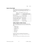
You can use these defaults or select other sources and destinations for the 
counter/timer signals in NI-DAQmx. Refer to 

Connecting Counter Signals


in the 

NI-DAQmx Help

 or the 

LabVIEW 8.x Help

 for more information on 

how to connect your signals for common counter measurements and 
generations. M Series default PFI lines for counter functions are listed in 

Physical Channels

 in the 

NI-DAQmx Help

 or the 

LabVIEW 8.x Help

.

Counter Triggering

Counters support three different triggering actions—arm start, start, and 
pause.

Arm Start Trigger

To begin any counter input or output function, you must first enable, or arm, 
the counter. Software can arm a counter or configure counters to be armed 
on a hardware signal. Software calls this hardware signal the Arm Start 
Trigger. Internally, software routes the Arm Start Trigger to the Counter 

n


HW Arm input of the counter.

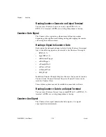
For counter output operations, you can use it in addition to the start and 
pause triggers. For counter input operations, you can use the arm start 
trigger to have start trigger-like behavior. The arm start trigger can be used 
for synchronizing multiple counter input and output tasks.

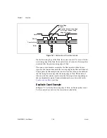
Start Trigger

For counter output operations, a start trigger can be configured to begin a 
finite or continuous pulse generation. When a continuous generation has 
triggered, the pulses continue to generate until you stop the operation in 
software. For finite generations, the specified number of pulses is generated 
and the generation stops unless you use the retriggerable attribute. When 
you use this attribute, subsequent start triggers cause the generation to 
restart.

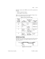
When using a start trigger, the start trigger source is routed to the Counter 

n

 Gate signal input of the counter.

Counter input operations can use the arm start trigger to have start 
trigger-like behavior.

Summary of Contents for NI 6232

Page 1: ...DAQ M Series NI 6232 6233 User Manual NI 6232 6233 User Manual July 2006 371995A 01 ...

Page 2: ...Korea 82 02 3451 3400 Lebanon 961 0 1 33 28 28 Malaysia 1800 887710 Mexico 01 800 010 0793 Netherlands 31 0 348 433 466 New Zealand 0800 553 322 Norway 47 0 66 90 76 60 Poland 48 22 3390150 Portugal 351 210 311 210 Russia 7 095 783 68 51 Singapore 1800 226 5886 Slovenia 386 3 425 4200 South Africa 27 0 11 805 8197 Spain 34 91 640 0085 Sweden 46 0 8 587 895 00 Switzerland 41 56 200 51 51 Taiwan 886...

Page 3: ...oduced or transmitted in any form electronic or mechanical including photocopying recording storing in an information retrieval system or translating in whole or in part without the prior written consent of National Instruments Corporation National Instruments respects the intellectual property of others and we ask our users to do the same NI software is protected by copyright and other intellectu...

Page 4: ...NATIONAL INSTRUMENTS PRODUCTS ARE INCORPORATED IN A SYSTEM OR APPLICATION INCLUDING WITHOUT LIMITATION THE APPROPRIATE DESIGN PROCESS AND SAFETY LEVEL OF SUCH SYSTEM OR APPLICATION ...

Page 5: ...nt of Communications DOC Changes or modifications not expressly approved by NI could void the user s authority to operate the equipment under the FCC Rules Class A Federal Communications Commission This equipment has been tested and found to comply with the limits for a Class A digital device pursuant to part 15 of the FCC Rules These limits are designed to provide reasonable protection against ha...

Page 6: ... NI Application Software xix Device Documentation and Specifications xix Training Courses xix Technical Support on the Web xix Chapter 1 Getting Started Installing NI DAQmx 1 1 Installing Other Software 1 1 Installing the Hardware 1 1 Device Pinouts 1 1 Device Specifications 1 2 Device Accessories and Cables 1 2 Chapter 2 DAQ System Overview DAQ Hardware 2 1 DAQ STC2 2 2 Calibration Circuitry 2 3 ...

Page 7: ...oid Scanning Faster Than Necessary 4 9 Example 1 4 9 Example 2 4 9 Analog Input Data Acquisition Methods 4 9 Software Timed Acquisitions 4 9 Hardware Timed Acquisitions 4 10 Buffered 4 10 Non Buffered 4 11 Analog Input Triggering 4 11 Connecting Analog Voltage Input Signals 4 11 Types of Signal Sources 4 12 Floating Signal Sources 4 13 Ground Referenced Signal Sources 4 13 Differential Connection ...

Page 8: ...rence Trigger Signal 4 29 Using a Digital Source 4 30 Routing AI Reference Trigger Signal to an Output Terminal 4 30 AI Pause Trigger Signal 4 30 Using a Digital Source 4 31 Routing AI Pause Trigger Signal to an Output Terminal 4 31 Getting Started with AI Applications in Software 4 31 Chapter 5 Analog Output Analog Output Circuitry 5 1 Minimizing Glitches on the Output Signal 5 2 Analog Output Da...

Page 9: ...s 7 3 Single Point On Demand Edge Counting 7 3 Buffered Sample Clock Edge Counting 7 4 Non Cumulative Buffered Edge Counting 7 5 Controlling the Direction of Counting 7 5 Pulse Width Measurement 7 6 Single Pulse Width Measurement 7 6 Buffered Pulse Width Measurement 7 7 Period Measurement 7 7 Single Period Measurement 7 8 Buffered Period Measurement 7 8 Semi Period Measurement 7 9 Single Semi Peri...

Page 10: ...Source Signal 7 27 Routing a Signal to Counter n Source 7 27 Routing Counter n Source to an Output Terminal 7 28 Counter n Gate Signal 7 28 Routing a Signal to Counter n Gate 7 28 Routing Counter n Gate to an Output Terminal 7 28 Counter n Aux Signal 7 28 Routing a Signal to Counter n Aux 7 29 Counter n A Counter n B and Counter n Z Signals 7 29 Routing Signals to A B and Z Counter Inputs 7 29 Rou...

Page 11: ... 8 2 Exporting Timing Output Signals Using PFI Terminals 8 3 Using PFI Terminals as Static Digital Inputs and Outputs 8 3 Connecting PFI Input Signals 8 3 PFI Filters 8 4 I O Protection 8 5 Programmable Power Up States 8 6 Connecting Digital I O Signals 8 6 Chapter 9 Isolation and Digital Isolators Digital Isolation 9 2 Benefits of an Isolated DAQ Device 9 2 Chapter 10 Digital Routing and Clock Ge...

Page 12: ...ntrollers 11 1 PXI Considerations 11 2 PXI Clock and Trigger Signals 11 2 PXI and PXI Express 11 2 Using PXI with CompactPCI 11 3 Data Transfer Methods 11 3 Direct Memory Access DMA 11 3 Interrupt Request IRQ 11 4 Programmed I O 11 4 Changing Data Transfer Methods between DMA and IRQ 11 4 Chapter 12 Triggering Triggering with a Digital Source 12 1 Appendix A Device Specific Information Appendix B ...

Page 13: ...ns directs you to pull down the File menu select the Page Setup item and select Options from the last dialog box This icon denotes a note which alerts you to important information This icon denotes a caution which advises you of precautions to take to avoid injury data loss or a system crash When this symbol is marked on a product refer to the NI 6232 6233 Specifcations for information about preca...

Page 14: ...stall your NI DAQmx for Windows software your NI DAQmx supported DAQ device and how to confirm that your device is operating properly Select Start All Programs National Instruments NI DAQ DAQ Getting Started Guide The NI DAQ Readme lists which devices are supported by this version of NI DAQ Select Start All Programs National Instruments NI DAQ NI DAQ Readme The NI DAQmx Help contains general infor...

Page 15: ... LabVIEW select Help NI DAQmx Base VI Reference Help The NI DAQmx Base C Reference Help contains C reference and general information about measurement concepts Select Start All Programs National Instruments NI DAQmx Base Documentation C Function Reference Manual LabVIEW If you are a new user use the Getting Started with LabVIEW manual to familiarize yourself with the LabVIEW graphical programming ...

Page 16: ...ant In LabWindows CVI select Help Contents then select Using LabWindows CVI Data Acquisition The NI DAQmx Library book of the LabWindows CVI Help contains API overviews and function reference for NI DAQmx Select Library Reference NI DAQmx Library in the LabWindows CVI Help Measurement Studio The NI Measurement Studio Help contains function reference measurement concepts and a walkthrough for using...

Page 17: ...evice using the Device Document Browser at any time by inserting the CD After installing the Device Document Browser device documents are accessible from Start All Programs National Instruments NI DAQ Browse Device Documentation Training Courses If you need more help getting started developing an application with NI products NI offers training courses To enroll in a course or obtain a detailed cou...

Page 18: ...ll the software you plan to use with the device Installing NI DAQmx The DAQ Getting Started Guide which you can download at ni com manuals offers NI DAQmx users step by step instructions for installing software and hardware configuring channels and tasks and getting started developing an application Installing Other Software If you are using other software refer to the installation instructions th...

Page 19: ...ifications available on the NI DAQ Device Document Browser or ni com manuals for more detailed information on the NI 6232 6233 device Device Accessories and Cables NI offers a variety of accessories and cables to use with your DAQ device Refer to Appendix A Device Specific Information or ni com for more information ...

Page 20: ...gramming software and a PC The following sections cover the components of a typical DAQ system Figure 2 1 Components of a Typical DAQ System DAQ Hardware DAQ hardware digitizes signals performs D A conversions to generate analog output signals and measures and controls digital I O signals Figure 2 2 features the components of the NI 6232 6233 device Sensors and Transducers DAQ Hardware Personal Co...

Page 21: ...FOs Generation and routing of RTSI signals for multi device synchronization Generation and routing of internal and external timing signals Two flexible 32 bit counter timer modules with hardware gating Static DIO signals PLL for clock synchronization PCI PXI interface Independent scatter gather DMA controllers for all acquisition and generation functions P1 GND P1 Analog Output Analog Input PFI St...

Page 22: ...nsors and Transducers Sensors can generate electrical signals to measure physical phenomena such as temperature force sound or light Some commonly used sensors are strain gauges thermocouples thermistors angular encoders linear encoders and resistance temperature detectors RTDs To measure signals from these various transducers you must convert them into a form that a DAQ device can accept For exam...

Page 23: ...lications However if you want to develop your own cable the following kits can assist you TB 37F 37SC 37 pin solder cup terminals shell with strain relief TB 37F 37CP 37 pin crimp poke terminals shell with strain relief Also adhere to the following guidelines for best results For AI signals use shielded twisted pair wires for each AI pair of differential inputs Connect the shield for each signal p...

Page 24: ...ftware configuration Refer to the DAQ Getting Started Guide for more information about the two drivers NI DAQmx includes a collection of programming examples to help you get started developing an application You can modify example code and save it in an application You can use examples to develop a new application or add example code to an existing application To locate LabVIEW and LabWindows CVI ...

Page 25: ...ND are isolated from earth ground chassis ground P0 GND and P1 GND AI 0 15 AI GND Input Analog Input Channels 0 to 15 For single ended measurements each signal is an analog input voltage channel In RSE mode AI GND is the reference for these signals For differential measurements AI 0 and AI 8 are the positive and negative inputs of differential analog input channel 0 Similarly the following signal ...

Page 26: ...these terminals can be individually configured as an output directional PFI terminal or a digital output terminal As a PFI output you can route many different internal AI or AO timing signals to each PFI terminal You also can route the counter timer outputs to each PFI terminal Note PFI 6 9 P1 0 3 are isolated from earth ground chassis ground AI GND AO GND and P0 GND NC No connect Do not connect s...

Page 27: ...ormation National Instruments Corporation 3 3 NI 6232 6233 User Manual RTSI Connector Pinout Refer to the RTSI Connector Pinout section of Chapter 10 Digital Routing and Clock Generation for information on the RTSI connector ...

Page 28: ...analog input signals depends on the analog input ground reference settings described in the Analog Input Ground Reference Settings section Also refer to Appendix A Device Specific Information for device I O connector pinouts MUX Each M Series device has one analog to digital converter ADC The multiplexers MUX route one AI channel at a time to the ADC through the NI PGIA DIFF RSE or NRSE I O Connec...

Page 29: ... to digital converter ADC digitizes the AI signal by converting the analog voltage into a digital number Isolation Barrier and Digital Isolators The digital isolators across the isolation barrier provide a ground break between the isolated analog front end and the earth chassis building ground AI FIFO M Series devices can perform both single and multiple A D conversions of a fixed or infinite numb...

Page 30: ... above would indicate Choose an input range that matches the expected input range of your signal A large input range can accommodate a large signal variation but reduces the voltage resolution Choosing a smaller input range improves the voltage resolution but may result in the input signal going out of range For more information on programming these settings refer to the NI DAQmx Help or the LabVI...

Page 31: ...erence in voltage between its two inputs The PGIA drives the ADC with this amplified voltage The amount of amplification the gain is determined by the analog input range as shown in Figure 4 2 Figure 4 2 PGIA Table 4 2 Analog Input Ground Reference Settings AI Ground Reference Settings Description DIFF In differential DIFF mode the NI 6232 6233 device measures the difference in voltage between two...

Page 32: ...um input voltage or maximum working voltage rating also can damage the device and the computer Exceeding the maximum input voltage can cause injury and harm the user NI is not liable for any damage or injuries resulting from such signal connections AI ground reference setting is sometimes referred to as AI terminal configuration Configuring AI Ground Reference Settings in Software You can program ...

Page 33: ...ge Settling time refers to the time it takes the NI PGIA to amplify the input signal to the desired accuracy before it is sampled by the ADC The NI 6232 6233 Specifications shows the device settling time M Series devices are designed to have fast settling times However several factors can increase the settling time which decreases the accuracy of your measurements To ensure fast settling times you...

Page 34: ...fo and entering the info code rdbbis Use Short High Quality Cabling Using short high quality cables can minimize several effects that degrade accuracy including crosstalk transmission line effects and noise The capacitance of the cable also can increase the settling time National Instruments recommends using individually shielded twisted pair wires that are 2 m or less to connect AI signals to the...

Page 35: ...is 10 V to 10 V and the input range of channel 1 is 200 mV to 200 mV You can connect channel 2 to AI GND or you can use the internal ground signal refer to Internal Channels in the NI DAQmx Help or the LabVIEW 8 x Help Set the input range of channel 2 to 200 mV to 200 mV to match channel 1 Then scan channels in the order 0 2 1 Inserting a grounded channel between signal channels improves settling ...

Page 36: ...are root of 2 However doubling the number of samples in this example decreases the time the PGIA has to settle from 4 µs to 2 µs In some cases the slower scan rate system returns more accurate results Example 2 If the time relationship between channels is not critical you can sample from the same channel multiple times and scan less frequently For example suppose an application requires averaging ...

Page 37: ...data is moved from the onboard FIFO memory of a DAQ device to a PC buffer using DMA or interrupts before it is transferred to application memory Buffered acquisitions typically allow for much faster transfer rates than non buffered acquisitions because data is moved in large blocks rather than one point at a time One property of buffered I O operations is the sample mode The sample mode can be eit...

Page 38: ...e Typically hardware timed non buffered operations are used to read single samples with known time increments between them and good latency Analog Input Triggering Analog input supports three different triggering actions Start trigger Reference trigger Pause trigger Refer to the AI Start Trigger Signal AI Reference Trigger Signal and AI Pause Trigger Signal sections for information on these trigge...

Page 39: ...ducts the front ends are isolated from the building ground system breaking any electrical connection between the Table 4 4 Analog Input Configuration Input Floating Signal Sources Not Connected to Building Ground Ground Referenced Signal Sources Examples Ungrounded thermocouples Signal conditioning with isolated outputs Battery devices Example Plug in instruments with non isolated outputs Differen...

Page 40: ...nd so you must connect the ground reference to AI GND to establish a local or onboard reference to the signal Non isolated outputs of instruments and devices that plug into the building power system fall into this category The difference in ground potential between an instrument and your PC connected to the same building power system is typically between 1 and 100 mV but the difference can be much...

Page 41: ...ease common mode noise rejection DIFF signal connections also allow input signals to float within the common mode limits of the PGIA Differential Connections for Ground Referenced Signal Sources Figure 4 4 shows how to connect a ground referenced signal source to a channel on the device configured in DIFF mode Figure 4 4 Differential Connections for Ground Referenced Signal Sources PGIA Vs AI GND ...

Page 42: ...cting the signal sources to the device The PGIA can reject common mode signals as long as AI and AI input signals are both within 11 V of AI GND Differential Input Biasing Figure 4 4 shows AI GND connected to the negative lead of the signal source If you do not connect AI GND the source is not likely to remain within the common mode signal range of the PGIA due to the floating source or the isolat...

Page 43: ...e the source to AI GND The easiest way to make this reference is to connect the positive side of the signal to the positive input of the PGIA and connect the negative side of the signal to AI GND as well as to the negative input of the PGIA without using resistors Single Ended Connection Considerations A single ended connection is one in which the device AI signal is referenced to a ground that it...

Page 44: ...nce point for all analog input signals but the reference ground plane is floating requiring the user to provide a reference ground An isolated device protects users against ground loops in their measurement as well as allowing the user to provide a reference ground that is not electrically connected to earth system or building ground In the single ended modes more electrostatic and magnetic noise ...

Page 45: ... PGIA can reject common mode signals as long as AI x input signal is within 11 V of AI GND Field Wiring Considerations Environmental noise can seriously affect the measurement accuracy of the device if you do not take proper care when running signal wires between signal sources and the device The following recommendations apply mainly to AI signal routing to the device although they also apply to ...

Page 46: ... the info code rdfwn3 Analog Input Timing Signals In order to provide all of the timing functionality described throughout this section NI 6232 6233 devices have a flexible timing engine Figure 4 7 summarizes all of the timing options provided by the analog input timing engine Also refer to the Clock Routing section of Chapter 10 Digital Routing and Clock Generation Figure 4 7 Analog Input Timing ...

Page 47: ...ock At this point NI DAQmx uses round robin channel sampling evenly dividing the time between scans by the number of channels being acquired to obtain the interchannel delay In this case you can calculate the Channel Clock by multiplying the scan rate by the number of channels being acquired For example the NI 623x M Series device has a maximum sampling rate of 250 kS s At a slower acquisition rat...

Page 48: ...ed DAQ sequence is shown in Figure 4 9 In this example the DAQ device reads two channels five times The sample counter is loaded with the specified number of posttrigger samples in this example five The value decrements with each pulse on ai SampleClock until the value reaches zero and all desired samples have been acquired Figure 4 9 Posttriggered Data Acquisition Example Pretriggered data acquis...

Page 49: ...se Signal AI Convert Clock Signal AI Convert Clock Timebase Signal AI Hold Complete Event Signal AI Start Trigger Signal AI Reference Trigger Signal AI Pause Trigger Signal AI Sample Clock Signal Use the AI Sample Clock ai SampleClock signal to initiate a set of measurements Your M Series device samples the AI signals of every channel in the task once for every ai SampleClock A measurement acquisi...

Page 50: ...FI 0 5 RTSI 0 7 PXI_STAR Routing AI Sample Clock Signal to an Output Terminal You can route ai SampleClock out to any output PFI 6 9 or RTSI 0 7 terminal This pulse is always active high You can specify the output to have one of two behaviors With the pulse behavior your DAQ device briefly pulses the PFI terminal once for every occurrence of ai SampleClock With level behavior your DAQ device drive...

Page 51: ...nts of ai ConvertClock Failure to do so may result in ai SampleClock pulses that are masked off and acquisitions with erratic sampling intervals Refer to the AI Convert Clock Signal section for more information on the timing requirements between ai ConvertClock and ai SampleClock Figure 4 11 shows the relationship of ai SampleClock to ai StartTrigger Figure 4 11 ai SampleClock and ai StartTrigger ...

Page 52: ...cheme enables the channels to approximate simultaneous sampling and still allow for adequate settling time If the AI Sample Clock rate is too fast to allow for this 10 µs of padding NI DAQmx will choose the conversion rate so that the AI Convert Clock pulses are evenly spaced throughout the sample To explicitly specify the conversion rate use the AI Convert Clock Rate DAQmx Timing property node or...

Page 53: ... terminals are fixed inputs PFI 6 9 terminals are fixed outputs Using a Delay from Sample Clock to Convert Clock When using an internally generated ai ConvertClock you also can specify a configurable delay from ai SampleClock to the first ai ConvertClock pulse within the sample By default this delay is three ticks of ai ConvertClockTimebase Figure 4 12 shows the relationship of ai SampleClock to a...

Page 54: ...receives another ai SampleClock Figure 4 13 shows timing sequences for a four channel acquisition using AI channels 0 1 2 and 3 and demonstrates proper and improper sequencing of ai SampleClock and ai ConvertClock It is also possible to use a single external signal to drive both ai SampleClock and ai ConvertClock at the same time In this mode each tick of the external clock will cause a conversion...

Page 55: ...ition A measurement acquisition consists of one or more samples If you do not use triggers begin a measurement with a software command When the acquisition begins configure the acquisition to stop under the following conditions When a certain number of points are sampled in finite mode After a hardware reference trigger in finite mode With a software command in continuous mode An acquisition that ...

Page 56: ...he reference trigger The number of posttrigger samples samples that occur after the reference trigger desired is the buffer size minus the number of pretrigger samples When the acquisition begins the DAQ device writes samples to the buffer After the DAQ device captures the specified number of pretrigger samples the DAQ device begins to look for the reference trigger condition If the reference trig...

Page 57: ...ion You also can specify whether the measurement acquisition stops on the rising edge or falling edge of ai ReferenceTrigger Routing AI Reference Trigger Signal to an Output Terminal You can route ai ReferenceTrigger out to any output PFI 6 9 or RTSI 0 7 terminal AI Pause Trigger Signal You can use the AI Pause Trigger ai PauseTrigger signal to pause and resume a measurement acquisition The intern...

Page 58: ...o an Output Terminal You can route ai PauseTrigger out to RTSI 0 7 Note Pause triggers are only sensitive to the level of the source not the edge Getting Started with AI Applications in Software You can use the M Series device in the following analog input applications Single point analog input Finite analog input Continuous analog input You can perform these applications through DMA interrupt or ...

Page 59: ...alog output circuitry of NI 6232 6233 devices Figure 5 1 NI 6232 6233 Analog Output Circuitry Analog Output Circuitry DACs Digital to analog converters DACs convert digital codes to analog voltages AO FIFO The AO FIFO enables analog output waveform generation It is a first in first out FIFO memory buffer between the computer and the AO Data AO Sample Clock AO 0 AO 1 DAC0 DAC1 AO FIFO Isolation Bar...

Page 60: ...ale transitions The largest glitches occur when the most significant bit of the DAC code changes You can build a lowpass deglitching filter to remove some of these glitches depending on the frequency and nature of the output signal Visit ni com support for more information on minimizing glitches Analog Output Data Generation Methods When performing an analog output operation you either can perform...

Page 61: ... between them and good latency Buffered In a buffered acquisition data is moved from a PC buffer to the onboard FIFO of the DAQ device using DMA or interrupts before it is written to the DACs one sample at a time Buffered acquisitions typically allow for much faster transfer rates than non buffered acquisitions because data is moved in large blocks rather than one point at a time One property of b...

Page 62: ... thereby preventing any problems that may occur due to excessive bus traffic With non regeneration old data will not be repeated New data must be continually written to the buffer If the program does not write new data to the buffer at a fast enough rate to keep up with the generation the buffer will underflow and cause an error Analog Output Triggering Analog output supports two different trigger...

Page 63: ...ser Manual Figure 5 2 Analog Output Connections Analog Output Timing Signals Figure 5 3 summarizes all of the timing options provided by the analog output timing engine Load Load V OUT V OUT AO 1 AO 0 Channel 1 Channel 0 I O Connector AO GND Isolation Barrier Digital Isolators ...

Page 64: ...art Trigger ao StartTrigger signal to initiate a waveform generation If you do not use triggers you can begin a generation with a software command Using a Digital Source To use ao StartTrigger specify a source and an edge The source can be one of the following signals A software pulse Input PFI 0 5 RTSI 0 7 ai ReferenceTrigger ai StartTrigger PXI_STAR PFI RTSI PXI_STAR 20 MHz Timebase 100 kHz Time...

Page 65: ...are fixed outputs AO Pause Trigger Signal Use the AO Pause Trigger signal ao PauseTrigger to mask off samples in a DAQ sequence That is when ao PauseTrigger is active no samples occur ao PauseTrigger does not stop a sample that is in progress The pause does not take effect until the beginning of the next sample When you generate analog output signals the generation pauses as soon as the pause trig...

Page 66: ...r to Device Routing in MAX in the NI DAQmx Help or the LabVIEW 8 x Help for more information You also can specify whether the samples are paused when ao PauseTrigger is at a logic high or low level Routing AO Pause Trigger Signal to an Output Terminal You can route ao PauseTrigger out to RTSI 0 7 AO Sample Clock Signal Use the AO Sample Clock ao SampleClock signal to initiate AO samples Each sampl...

Page 67: ...ample Clock Signal to an Output Terminal You can route ao SampleClock as an active low signal out to any output PFI 6 9 or RTSI 0 7 terminal Other Timing Requirements A counter on your device internally generates ao SampleClock unless you select some external source ao StartTrigger starts the counter and either the software or hardware can stop it when a finite generation completes When using an i...

Page 68: ... 0 5 RTSI 0 7 PXI_STAR ao SampleClockTimebase is not available as an output on the I O connector You might use ao SampleClockTimebase if you want to use an external sample clock signal but need to divide the signal down If you want to use an external sample clock signal but do not need to divide the signal then you should use ao SampleClock rather than ao SampleClockTimebase Getting Started with A...

Page 69: ...veform generation You can perform these generations through programmed I O interrupt or DMA data transfer mechanisms Some of the applications also use start triggers and pause triggers Note For more information about programming analog output applications and triggers in software refer to the NI DAQmx Help or the LabVIEW 8 x Help ...

Page 70: ...put line to any external signal source ground signal or power supply Understand the current requirements of the load connected to the digital output lines Do not exceed the specified current output limits of the digital outputs NI has several signal conditioning solutions for digital applications requiring high current drive Do not drive the digital input lines with voltages or current outside of ...

Page 71: ... 3 are referenced to P1 GND Figures 6 1 and 6 2 show P0 0 5 and P1 0 3 on the NI 6232 and the NI 6233 device respectively Digital input and output signals can range from 0 to 30 V Refer to the NI 6232 6233 Specifications for more information Figure 6 1 NI 6232 Digital I O Connections DO Source P1 0 3 P1 VCC P1 0 P1 1 P1 GND P0 0 P0 GND P1 GND P0 GND Digital Isolators ...

Page 72: ...s which are listed in the NI 6232 6233 Specifications can damage the DAQ device and the computer NI is not liable for any damage resulting from such signal connections Logic Conventions With NI 6232 6233 devices logic 0 means that the Darlington output switch is open while logic 1 means closed Table 6 1 summarizes the expected behavior P1 0 3 P1 0 P1 VCC P1 GND P1 1 P1 GND P0 0 P0 GND P0 GND P1 GN...

Page 73: ...es in the following digital I O applications Static digital input Static digital output Note For more information about programming digital I O applications and triggers in software refer to the NI DAQmx Help or the LabVIEW 8 x Help Table 6 1 NI 6232 6233 Logic Conventions Device Logic 0 1 NI 6232 Source DO P1 GND P1 VCC NI 6233 Sink DO P1 VCC P1 GND ...

Page 74: ... and one frequency generator as shown in Figure 7 1 The general purpose counter timers can be used for many measurement and pulse generation applications Caution When making measurements take into account the minimum pulse width and time delay of the digital input and output lines Refer to the NI 6238 6239 Specifications for more information ...

Page 75: ...0 Counter 0 Source Counter 0 Timebase Counter 0 Aux Counter 0 HW Arm Counter 0 A Counter 0 B Counter 0 Up_Down Counter 0 Z Counter 0 Gate Counter 0 Internal Output Counter 0 TC Input Selection Muxes Frequency Generator Frequency Output Timebase Freq Out Input Selection Muxes Counter 1 Counter 1 Source Counter 1 Timebase Counter 1 Aux Counter 1 HW Arm Counter 1 A Counter 1 B Counter 1 Up_Down Count...

Page 76: ...input after the counter is armed On demand refers to the fact that software can read the counter contents at any time without disturbing the counting process Figure 7 2 shows an example of single point edge counting Figure 7 2 Single Point On Demand Edge Counting You also can use a pause trigger to pause or gate the counter When the pause trigger is active the counter ignores edges on its Source i...

Page 77: ...returned are the cumulative counts since the counter armed event That is the sample clock does not reset the counter You can route the counter sample clock to the Gate input of the counter You can configure the counter to sample on the rising or falling edge of the sample clock Figure 7 4 shows an example of buffered edge counting Notice that counting begins when the counter is armed which occurs ...

Page 78: ... edge on Gate Notice that if you are using an external signal as the Source at least one Source pulse should occur between each active edge of the Gate signal This condition ensures that correct values are returned by the counter If this condition is not met consider using duplicate count prevention Controlling the Direction of Counting In edge counting applications the counter can count up or dow...

Page 79: ...the number of edges returned by the counter A pulse width measurement will be accurate even if the counter is armed while a pulse train is in progress If a counter is armed while the pulse is in the active state it will wait for the next transition to the active state to begin the measurement Single Pulse Width Measurement With single pulse width measurement the counter counts the number of edges ...

Page 80: ...ment Note that if you are using an external signal as the Source at least one Source pulse should occur between each active edge of the Gate signal This condition ensures that correct values are returned by the counter If this condition is not met consider using duplicate count prevention For information on connecting counter signals refer to the Default Counter Terminals section Period Measuremen...

Page 81: ...example of a single period measurement Figure 7 8 Single Period Measurement Buffered Period Measurement Buffered period measurement is similar to single period measurement but buffered period measurement measures multiple periods The counter counts the number of rising or falling edges on the Source input between each pair of active edges on the Gate input At the end of each period on the Gate sig...

Page 82: ...nter measures a semi period on its Gate input signal after the counter is armed A semi period is the time between any two consecutive edges on the Gate input You can route an internal or external periodic clock signal with a known period to the Source input of the counter The counter counts the number of rising or falling edges occurring on the Source input between two edges of the Gate signal You...

Page 83: ...emi Period Measurement Note that if you are using an external signal as the Source at least one Source pulse should occur between each active edge of the Gate signal This condition ensures that correct values are returned by the counter If this condition is not met consider using duplicate count prevention For information on connecting counter signals refer to the Default Counter Terminals section...

Page 84: ...several periods of your signal using a known timebase This method is good for low to medium frequency signals You can route the signal to measure F1 to the Gate of a counter You can route a known timebase Ft to the Source of the counter The known timebase can be 80MHzTimebase For signals that might be slower than 0 02 Hz use a slower known timebase You can configure the counter to make K 1 buffere...

Page 85: ...an generate the pulse externally and connect it to a PFI or RTSI terminal You only need to use one counter if you generate the pulse externally Route the signal to measure F1 to the Source of the counter Configure the counter for a single pulse width measurement Suppose you measure the width of pulse T to be N periods of F1 Then the frequency of F1 is N T Figure 7 13 illustrates this method Anothe...

Page 86: ...long pulse using the signal to measure You then measure the long pulse with a known timebase The M Series device can measure this long pulse more accurately than the faster input signal You can route the signal to measure to the Source input of Counter 0 as shown in Figure 7 14 Assume this signal to measure has frequency F1 Configure Counter 0 to generate a single pulse that is the width of N peri...

Page 87: ...s N F1 From Counter 1 the length of the same pulse is J F2 Therefore the frequency of F1 is given by F1 F2 N J Choosing a Method for Measuring Frequency The best method to measure frequency depends on several factors including the expected frequency of the signal to measure the desired accuracy how many counters are available and how long the measurement can take Method 1 uses only one counter It ...

Page 88: ...gnals However the accuracy decreases as the frequency of the signal to measure decreases At very low frequencies Method 2 may be too inaccurate for your application Another disadvantage of Method 2 is that it requires two counters if you cannot provide an external signal of known width An advantage of Method 2 is that the measurement completes in a known amount of time Method 3 measures high and l...

Page 89: ...X1 X2 or X4 encoding A quadrature encoder can have up to three channels channels A B and Z X1 Encoding When channel A leads channel B in a quadrature cycle the counter increments When channel B leads channel A in a quadrature cycle the counter decrements The amount of increments and decrements per cycle depends on the type of encoding X1 X2 or X4 Figure 7 15 shows a quadrature cycle and the result...

Page 90: ...ing Whether the counter increments or decrements depends on which channel leads the other Each cycle results in four increments or decrements as shown in Figure 7 17 Figure 7 17 X4 Encoding Channel Z Behavior Some quadrature encoders have a third channel channel Z which is also referred to as the index channel A high level on channel Z causes the counter to be reloaded with a specified value in a ...

Page 91: ...is true and channel Z is high Incrementing and decrementing takes priority over reloading Thus when the channel B goes low to enter the reload phase the increment occurs first The reload occurs within one maximum timebase period after the reload phase becomes true After the reload occurs the counter continues to count as before Figure 7 18 illustrates channel Z reload with X4 decoding Figure 7 18 ...

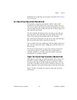
Page 92: ...ctive edge on the Gate input The counter stores the count in a hardware save register You can configure the rising or falling edge of the Aux input to be the active edge You can configure the rising or falling edge of the Gate input to be the active edge Use this type of measurement to count events or measure the time that occurs between edges on two signals This type of measurement is sometimes r...

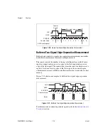
Page 93: ...e of the Aux signal The counter then stores the count in a hardware save register On the next active edge of the Gate signal the counter begins another measurement A DMA controller transfers the stored values to host memory Figure 7 21 shows an example of a buffered two signal edge separation measurement Figure 7 21 Buffered Two Signal Edge Separation Measurement For information on connecting coun...

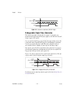
Page 94: ... of a pulse with a pulse delay of four and a pulse width of three using the rising edge of Source Figure 7 22 Single Pulse Generation Single Pulse Generation with Start Trigger The counter can output a single pulse in response to one pulse on a hardware Start Trigger signal The pulse appears on the Counter n Internal Output signal of the counter You can route the Start Trigger signal to the Gate i...

Page 95: ...lse You also can specify the pulse width The delay and pulse width are measured in terms of a number of active edges of the Source input The counter ignores the Gate input while a pulse generation is in progress After the pulse generation is finished the counter waits for another Start Trigger signal to begin another pulse generation Figure 7 24 shows a generation of two pulses with a pulse delay ...

Page 96: ...or falling The counter can begin the pulse train generation as soon as the counter is armed or in response to a hardware Start Trigger You can route the Start Trigger to the Gate input of the counter You also can use the Gate input of the counter as a Pause Trigger if it is not used as a Start Trigger The counter pauses pulse generation when the Pause Trigger is active Figure 7 25 shows a continuo...

Page 97: ... Frequency Output signal The Frequency Output signal is the Frequency Output Timebase divided by a number you select from 1 to 16 The Frequency Output Timebase can be either the 20 MHz Timebase divided by 2 or the 100 kHz Timebase The duty cycle of Frequency Output is 50 if the divider is either 1 or an even number For an odd divider suppose the divider is set to D In this case Frequency Output is...

Page 98: ...tween the Gate and the pulse on the output by a specified amount Thus the delay between the Gate and the pulse produced successively increases Note ETS Equivalent Time Sampling The increase in the delay value can be between 0 and 255 For instance if you specify the increment to be 10 the delay between the active Gate edge and the pulse on the output will increase by 10 every time a new pulse is ge...

Page 99: ... the Default Counter Terminals section Counter Timing Signals M Series devices feature the following counter timing signals Counter n Source Counter n Gate Counter n Aux Counter n A Counter n B Counter n Z Counter n Up_Down Counter n HW Arm Counter n Internal Output Counter n TC Frequency Output In this section n refers to either Counter 0 or 1 For example Counter n Source refers to two signals Co...

Page 100: ... routed to the Counter n Source input 80 MHz Timebase 20 MHz Timebase 100 kHz Timebase RTSI 0 7 Input PFI 0 5 PXI_CLK10 PXI_STAR In addition Counter 1 TC or Counter 1 Gate can be routed to Counter 0 Source Counter 0 TC or Counter 0 Gate can be routed to Counter 1 Source Some of these options may not be available in some driver software Table 7 3 Counter Applications and Counter n Source Applicatio...

Page 101: ...n Gate signal Any of the following signals can be routed to the Counter n Gate input RTSI 0 7 Input PFI 0 5 ai ReferenceTrigger ai StartTrigger ai SampleClock ai ConvertClock ao SampleClock PXI_STAR In addition Counter 1 Internal Output or Counter 1 Source can be routed to Counter 0 Gate Counter 0 Internal Output or Counter 0 Source can be routed to Counter 1 Gate Some of these options may not be ...

Page 102: ...e can be routed to Counter 1 Aux Some of these options may not be available in some driver software Counter n A Counter n B and Counter n Z Signals Counter n B can control the direction of counting in edge counting applications Use the A B and Z inputs to each counter when measuring quadrature encoders or measuring two pulse encoders Routing Signals to A B and Z Counter Inputs Each counter has ind...

Page 103: ... this hardware signal the Arm Start Trigger Internally software routes the Arm Start Trigger to the Counter n HW Arm input of the counter Routing Signals to Counter n HW Arm Input Any of the following signals can be routed to the Counter n HW Arm input RTSI 0 7 Input PFI 0 5 ai ReferenceTrigger ai StartTrigger PXI_STAR Counter 1 Internal Output can be routed to Counter 0 HW Arm Counter 0 Internal ...

Page 104: ...utput to any output PFI 6 9 terminal All PFIs are set to high impedance at startup Default Counter Terminals By default NI DAQmx routes the counter timer inputs and outputs to the PFI pins shown in Table 7 4 Table 7 4 NI 6232 6233 Device Default NI DAQmx Counter Timer Pins Counter Timer Signal Default Pin Number Name Port CTR 0 SRC 13 PFI 0 P0 0 CTR 0 GATE 32 PFI 1 P0 1 CTR 0 AUX 33 PFI 2 P0 2 CTR...

Page 105: ...oftware routes the Arm Start Trigger to the Counter n HW Arm input of the counter For counter output operations you can use it in addition to the start and pause triggers For counter input operations you can use the arm start trigger to have start trigger like behavior The arm start trigger can be used for synchronizing multiple counter input and output tasks Start Trigger For counter output opera...

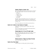
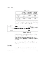
Page 106: ...it counter By cascading counters you also can enable other applications For example to improve the accuracy of frequency measurements use reciprocal frequency measurement as described in the Method 3 Measure Large Range of Frequencies Using Two Counters section Counter Filters You can enable a programmable debouncing filter on each PFI RTSI or PXI_STAR signal When the filters are enabled your devi...

Page 107: ...rsion of the input signal Refer to the KnowledgeBase document Digital Filtering with M Series and CompactDAQ for more information about digital filters and counters To access this KnowledgeBase go to ni com info and enter the info code rddfms Prescaling Prescaling allows the counter to count a signal that is faster than the maximum timebase of the counter M Series devices offer 8X and 2X Table 7 5...

Page 108: ...llover Prescaling can be used for event counting provided it is acceptable to have an error of up to seven or one Prescaling can be used when the counter Source is an external signal Prescaling is not available if the counter Source is one of the internal timebases 80MHzTimebase 20MHzTimebase or 100kHzTimebase Duplicate Count Prevention Duplicate count prevention or synchronous counting mode ensur...

Page 109: ...te until the next Source pulse In this example the counter stores the values in the buffer on the first rising Source edge after the rising edge of Gate The details of when exactly the counter synchronizes the Gate signal vary depending on the synchronization mode Synchronization modes are described in the Synchronization Modes section Duplicate Count Example In Figure 7 32 after the first rising ...

Page 110: ...ate even if the Source does not pulse This enables the correct current count to be stored in the buffer even if no Source edges occur between Gate signals as shown in Figure 7 33 Figure 7 33 Duplicate Count Prevention Example Even if the Source pulses are long the counter increments only once for each Source pulse Gate Source Counter Value Buffer 7 6 7 1 No Source edge so no value written to buffe...

Page 111: ...20 MHz or less You can have the counter value and output to change synchronously with the 80 MHz Timebase In all other cases you should not use duplicate count prevention Enabling Duplicate Count Prevention in NI DAQmx You can enable duplicate count prevention in NI DAQmx by setting the Enable Duplicate Count Prevention attribute property For specific information on finding the Enable Duplicate Co...

Page 112: ...nals on the rising edge of the source and counts on the following rising edge of the source as shown in Figure 7 34 Figure 7 34 80 MHz Source Mode Table 7 6 Synchronization Mode Conditions Duplicate Count Prevention Enabled Type of Measurement SignalDriving Counter n Source Synchronizati on Mode Yes Any Any 80 MHz Source No Position Measurement Any 80 MHz Source No Any 80 MHz Timebase 80 MHz Sourc...

Page 113: ...igure 7 35 Figure 7 35 Other Internal Source Mode External Source Mode In external source mode the device generates a delayed Source signal by delaying the Source signal by several nanoseconds The device synchronizes signals on the rising edge of the delayed Source signal and counts on the following rising edge of the source as shown in Figure 7 36 Figure 7 36 External Source Mode Source Synchroni...

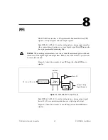
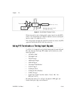
Page 114: ... into account the minimum pulse width and time delay of the digital input and output lines Refer to the NI 6238 6239 Specifications for more information Figure 8 1 shows the circuitry of one PFI input line Each PFI line is similar Figure 8 1 NI 6232 6233 PFI Input Circuitry Each PFI 6 9 P1 0 3 can be configured as a timing output signal from AI AO or counter timer functions or a static digital out...

Page 115: ...s to route external timing signals to many different M Series functions Each input PFI terminal can be routed to any of the following signals AI Convert Clock AI Sample Clock AI Start Trigger AI Reference Trigger AI Pause Trigger AI Sample Clock Timebase AO Start Trigger AO Sample Clock AO Sample Clock Timebase AO Pause Trigger Counter input signals for either counter Source Gate Aux HW_Arm A B Z ...

Page 116: ... observable by the user or another instrument Refer to the Digital Output Port 1 section of the NI 6232 6233 Specifications for more information Using PFI Terminals as Static Digital Inputs and Outputs When a terminal is used as a static digital input or output it is called P0 x or P1 x On the I O connector each terminal is labeled PFI x P0 x or PFI x P1 x Connecting PFI Input Signals All PFI inpu...

Page 117: ...Note NI DAQmx supports only filters on counter inputs The following is an example of low to high transitions of the input signal High to low transitions work similarly Assume that an input terminal has been low for a long time The input terminal then changes from low to high but glitches several times When the filter clock has sampled the signal high on N consecutive edges the low to high transiti...

Page 118: ...ltered version of the input signal Refer to the KnowledgeBase document Digital Filtering with M Series and CompactDAQ for more information about digital filters and counters To access this KnowledgeBase go to ni com info and enter the info code rddfms I O Protection Each DI DO and PFI signal is protected against overvoltage and undervoltage conditions as well as ESD events on NI 6232 6233 devices ...

Page 119: ...ide of its normal operating range Treat the DAQ device as you would treat any static sensitive device Always properly ground yourself and the equipment when handling the DAQ device or connecting to it Programmable Power Up States By default the digital output lines P1 0 3 PFI 6 9 are set to 0 They can be programmed to power up as 0 or 1 Refer to the NI DAQmx Help or the LabVIEW 8 x Help for more i...

Page 120: ...hapter 8 PFI National Instruments Corporation 8 7 NI 6232 6233 User Manual Figure 8 5 NI 6232 Digital I O Connections DO Source P1 0 3 P1 VCC P1 0 P1 1 P1 GND P0 0 P0 GND P1 GND P0 GND Digital Isolators ...

Page 121: ...ng the maximum input voltage or maximum working voltage ratings which are listed in the NI 6232 6233 Specifications can damage the DAQ device and the computer NI is not liable for any damage resulting from such signal connections P1 0 3 P1 0 P1 VCC P1 GND P1 1 P1 GND P0 0 P0 GND P0 GND P1 GND Digital Isolators Buffer ...

Page 122: ...rcuitry RTSI digital routing and clock generation are all referenced to a non isolated ground Refer to Table 9 1 for an example of the symbols for isolated ground and non isolated ground Figure 9 1 General NI 6232 6233 Block Diagram Table 9 1 Ground Symbols Isolated Ground Non Isolated Ground P1 GND P1 Analog Output Analog Input PFI Static DI PFI Static DO Digital Routing and Clock Generation Bus ...

Page 123: ...ors digital isolators do not introduce any analog error in the measurements taken by the device The A D converter used for analog input is on the isolated side of the device The analog inputs are digitized before they are sent across the isolation barrier Similarly the D A converters used for analog output are on the isolated side of the device Benefits of an Isolated DAQ Device With isolation eng...

Page 124: ...The acquisition generation sub systems use these signals to manage acquisitions and generations These signals can come from the following sources Your M Series device Other devices in your system through RTSI User input through the PFI terminals User input through the PXI_STAR terminal Routes and generates the main clock signals for the M Series device Clock Routing Figure 10 1 shows the clock rou...

Page 125: ...he 80 MHz Timebase 100 kHz Timebase The 100 kHz Timebase can be used to generate many of the AI and AO timing signals The 100 kHz Timebase also can be used as the Source input to the 32 bit general purpose counter timers The 100 kHz Timebase is generated by dividing down the 20 MHz Timebase by 200 External Reference Clock The external reference clock can be used as a source for the internal timeba...

Page 126: ...he initiator device receive the 10 MHz Reference Clock from RTSI This signal becomes the external reference clock A PLL on each device generates the internal timebases synchronous to the external reference clock On PXI systems you also can synchronize devices to PXI_CLK10 In this application the PXI chassis acts as the initiator Each PXI module routes PXI_CLK10 to its external reference clock Anot...

Page 127: ...ny as five DAQ vision motion or CAN devices in the computer In a PXI system the RTSI bus consists of the RTSI bus interface and the PXI trigger signals on the PXI backplane This bus can route timing and trigger signals between several functions on as many as seven DAQ devices in the system RTSI Connector Pinout Figure 10 2 shows the RTSI connector pinout and Table 10 1 describes the RTSI signals T...

Page 128: ...rigger ao SampleClock ao StartTrigger ao PauseTrigger 10 MHz Reference Clock Counter n Source Gate Z Internal Output FREQ OUT Input PFI 0 5 Note Signals with a are inverted before being driven on the RTSI terminals Table 10 1 RTSI Signal Descriptions RTSI Bus Signal Terminal RTSI 7 34 RTSI 6 32 RTSI 5 30 RTSI 4 28 RTSI 3 26 RTSI 2 24 RTSI 1 22 RTSI 0 20 Not Connected Do not connect signals to thes...

Page 129: ...e input is edge or level sensitive RTSI Filters You can enable a programmable debouncing filter on each PFI RTSI or PXI_STAR signal When the filters are enabled your device samples the input on each rising edge of a filter clock M Series devices use an onboard oscillator to generate the filter clock with a 40 MHz frequency Note NI DAQmx supports only filters on counter inputs The following is an e...

Page 130: ...ly to RTSI or a RTSI input is routed directly to PFI the M Series device does not use the filtered version of the input signal Refer to the KnowledgeBase document Digital Filtering with M Series and CompactDAQ for more information about digital filters and counters To access this KnowledgeBase go to ni com info and enter the info code rddfms Table 10 2 Filters Filter Setting N Filter ClocksNeeded ...

Page 131: ... peripheral modules On M Series devices the eight PXI trigger signals are synonymous with RTSI 0 7 Note that in a PXI chassis with more than eight slots the PXI trigger lines may be divided into multiple independent buses Refer to the documentation for your chassis for details PXI_STAR Trigger In a PXI system the Star Trigger bus implements a dedicated trigger line between the first peripheral slo...

Page 132: ...of low to high transitions of the input signal High to low transitions work similarly Assume that an input terminal has been low for a long time The input terminal then changes from low to high but glitches several times When the filter clock has sampled the signal high on N consecutive edges the low to high transition is propagated to the rest of the circuit The value of N depends on the filter s...

Page 133: ...rectly to RTSI or a RTSI input is routed directly to PFI the M Series device does not use the filtered version of the input signal Refer to the KnowledgeBase document Digital Filtering with M Series and CompactDAQ for more information about digital filters and counters To access this KnowledgeBase go to ni com info and enter the info code rddfms 1 2 3 1 4 1 2 3 4 5 RTSI PFI or PXI_STAR Terminal Fi...

Page 134: ...erface DMA Controllers NI 6232 6233 devices have four fully independent DMA controllers for high performance transfers of data blocks One DMA controller is available for each measurement and acquisition block Analog input Analog output Counter 0 Counter 1 Each DMA controller channel contains a FIFO and independent processes for filling and emptying the FIFO This allows the buses involved in the tr...

Page 135: ...chassis PXI specifications are developed by the PXI System Alliance www pxisa org Using the terminology of the PXI specifications NI PXI 6232 6233 devices are 3U Hybrid Slot Compatible PXI 1 Peripheral Modules 3U designates devices that are 100 mm tall as opposed to the taller 6U modules Hybrid slot compatible defines where the device can be installed PXI 6232 6233 devices can be installed in the ...

Page 136: ...CI chassis adhering to the PICMG CompactPCI 2 0 R3 0 core specification PXI specific features are implemented on the J2 connector of the CompactPCI bus The PXI device is compatible with any CompactPCI chassis with a sub bus that does not drive the lines used by that device Even if the sub bus is capable of driving these lines the PXI device is still compatible as long as those terminals on the sub...

Page 137: ...nism where the user s program is responsible for transferring data Each read or write call in the program initiates the transfer of data Programmed I O is typically used in software timed on demand operations Refer to the Software Timed Generations section of Chapter 5 Analog Output for more information Changing Data Transfer Methods between DMA and IRQ On PCI or PXI M Series devices each measurem...

Page 138: ...log Output Triggering section of Chapter 5 Analog Output The Counter Triggering section of Chapter 7 Counters Triggering with a Digital Source Your DAQ device can generate a trigger on a digital signal You must specify a source and an edge The digital source can be any of the PFI RTSI or PXI_STAR signals The edge can be either the rising edge or falling edge of the digital signal A rising edge is ...

Page 139: ...Chapter 12 Triggering NI 6232 6233 User Manual 12 2 ni com Analog output generation Counter behavior ...

Page 140: ...sory choices and other information for the NI 6232 and NI 6233 M Series isolated devices To obtain documentation for devices not listed here refer to ni com manuals NI 6232 NI 6232 Pinout Figure A 1 shows the pinout of the NI 6232 For a detailed description of each signal refer to the I O Connector Signal Descriptions section of Chapter 3 Connector Information ...

Page 141: ... PFI 1 P0 1 CTR 0 B 33 PFI 2 P0 2 CTR 1 SRC 15 PFI 3 P0 3 CTR 1 GATE 34 PFI 4 P0 4 CTR 1 AUX 16 PFI 5 P0 5 AI 0 AI 9 AI GND AI 10 AI 3 AI 4 NC NC AO 1 PFI 0 P0 0 Input P0 GND PFI 3 P0 3 Input PFI 5 P0 5 Input PFI 6 P1 0 Output PFI 8 P1 2 Output P1 GND AI 8 AI 1 AI 2 AI 11 AI GND AI 12 PFI 1 P0 1 Input PFI 2 P0 2 Input PFI 4 P0 4 Input P1 VCC PFI 7 P1 1 Output PFI 8 P1 3 Output NC No Connect 20 21 ...

Page 142: ...screw terminal connector blocks Use an SH37F 37M cable to connect an NI 6232 device to a connector block such as the following CB 37F HVD 37 pin DIN rail screw terminal block UL Recognized derated to 30 Vrms 42 4 Vpk or 60 VDC CB 37FH Horizontal DIN mountable terminal block with 37 screw terminals CB 37FV Vertical DIN mountable terminal block with 37 screw terminals CB 37F LP Low profile terminal ...

Page 143: ...cable UL Listed derated to 30 Vrms 42 4 Vpk or 60 VDC R37F 37M 1 37 pin female to male ribbon I O cable SH37F P 4 37 pin female to pigtails shielded I O cable Custom Cabling and Connectivity Refer to the Custom Cabling section of Chapter 2 DAQ System Overview for more information about custom cabling solutions NI 6233 NI 6233 Pinout Figure A 2 shows the pinout of the NI 6233 For a detailed descrip...

Page 144: ... 0 CTR 0 Z 32 PFI 1 P0 1 CTR 0 B 33 PFI 2 P0 2 CTR 1 SRC 15 PFI 3 P0 3 CTR 1 GATE 34 PFI 4 P0 4 CTR 1 AUX 16 PFI 5 P0 5 AI 0 AI 9 AI GND AI 10 AI 3 AI 4 NC NC AO 1 PFI 0 P0 0 Input P0 GND PFI 3 P0 3 Input PFI 5 P0 5 Input PFI 6 P1 0 Output PFI 8 P1 2 Output P1 VCC AI 8 AI 1 AI 2 AI 11 AI GND AI 12 PFI 1 P0 1 Input PFI 2 P0 2 Input PFI 4 P0 4 Input P1 GND PFI 7 P1 1 Output PFI 8 P1 3 Output NC No C...

Page 145: ...connector blocks Use an SH37F 37M cable to connect an NI 6233 device to a connector block such as the following CB 37F HVD 37 pin DIN rail screw terminal block UL Recognized derated to 30 Vrms 42 4 Vpk or 60 VDC CB 37FH Horizontal DIN mountable terminal block with 37 screw terminals CB 37FV Vertical DIN mountable terminal block with 37 screw terminals CB 37F LP Low profile terminal block with 37 s...

Page 146: ...red Cables In most applications you can use the following cables SH37F 37M x 37 pin female to male shielded I O cable UL Listed derated to 30 Vrms 42 4 Vpk or 60 VDC R37F 37M 1 37 pin female to male ribbon I O cable SH37F P 4 37 pin female to pigtails shielded I O cable Custom Cabling and Connectivity Refer to the Custom Cabling section of Chapter 2 DAQ System Overview for more information about c...

Page 147: ...connected to AI 1 is high enough the resulting reading can somewhat affect the voltage in AI 0 To circumvent this problem use a voltage follower that has operational amplifiers op amps with unity gain for each high impedance source before connecting to an M Series device Otherwise you must decrease the sample rate for each channel Another common cause of channel crosstalk is due to sampling among ...

Page 148: ...s section of Chapter 4 Analog Input for more information How can I use the AI Sample Clock and AI Convert Clock signals on an M Series device to sample the AI channel s M Series devices use ai SampleClock and ai ConvertClock to perform interval sampling As Figure B 1 shows ai SampleClock controls the sample period which is determined by the following equation 1 sample period sample rate Figure B 1...

Page 149: ...some of these glitches depending on the frequency and nature of the output signal Visit ni com support for more information on minimizing glitches Counters When multiple sample clocks on my buffered counter measurement occur before consecutive edges on my source I see weird behavior Why Duplicate count prevention ensures that the counter returns correct data for counter measurement in some applica...

Page 150: ...Instruments Application Engineers make sure every question receives an answer For information about other technical support options in your area visit ni com services or contact your local office at ni com contact Training and Certification Visit ni com training for self paced training eLearning virtual classrooms interactive CDs and Certification program information You also can register for inst...

Page 151: ...com calibration If you searched ni com and could not find the answers you need contact your local office or NI corporate headquarters Phone numbers for our worldwide offices are listed at the front of this manual You also can visit the Worldwide Offices section of ni com niglobal to access the branch office Web sites which provide up to date contact information support phone numbers email addresse...

Page 152: ... Per º Degree Ω Ohm A A Amperes the unit of electric current A D Analog to Digital Most often used as A D converter AC Alternating current accuracy A measure of the capability of an instrument or sensor to faithfully indicate the value of the measured signal This term is not related to resolution however the accuracy level can never be better than the resolution of the instrument ADE Application d...

Page 153: ...specific level on either an increasing or a decreasing signal positive or negative slope Analog triggering can be implemented either in software or in hardware When implemented in software LabVIEW all data is collected transferred into system memory and analyzed for the trigger condition When analog triggering is implemented in hardware no data is transferred to system memory until the trigger con...

Page 154: ...of a program or algorithm BNC Bayonet Neill Concelman A type of coaxial connector used in situations requiring shielded cable for signal connections and or controlled impedance applications buffer 1 Temporary storage for acquired or generated data 2 A memory device that stores intermediate data between two devices bus buses The group of electrical conductors that interconnect individual circuitry ...

Page 155: ...onic noise pick up that is common to both the positive and negative polarities of the input leads to the instrument front end Common mode rejection is only a relevant specification for systems having a balanced or differential input common mode signal 1 Any voltage present at the instrumentation amplifier inputs with respect to amplifier ground 2 The signal relative to the instrument chassis or co...

Page 156: ...g electrical signals from sensors transducers and test probes or fixtures and inputting them to a computer for processing 2 Data acquisition The process of collecting and measuring the same kinds of electrical signals with A D and or DIO devices plugged into a computer and possibly generating control signals with D A and or DIO devices in the same computer DAQ device A device that acquires or gene...

Page 157: ...speaks of current many different types of DC measurements are made including DC Voltage DC current and DC power device A plug in data acquisition product card or pad that can contain multiple channels and conversion devices Plug in products PCMCIA cards and devices such as the DAQPad 1200 which connects to your computer parallel port are all examples of DAQ devices SCXI modules are distinct from d...

Page 158: ... and I O devices independently of the CPU driver Software unique to the device or type of device and includes the set of commands the device accepts E edge detection A technique that locates an edge of an analog signal such as the edge of a square wave EEPROM Electrically Erasable Programmable Read Only Memory ROM that can be erased with an electrical signal and reprogrammed Some SCXI modules cont...

Page 159: ...ata can be stored on the FIFO ahead of time This again reduces the effect of latencies associated with getting the data from system memory to the DAQ device filter A physical device or digital algorithm that selectively removes noise from a signal or emphasizes certain frequency ranges and de emphasizes others Electronic filters include lowpass band pass and highpass types Digital filters can oper...

Page 160: ... A common reference point for an electrical system H hardware The physical components of a computer system such as the circuit boards plug in devices chassis enclosures peripherals and cables hardware triggering A form of triggering where you set the start time of an acquisition and gather data at a known position in time relative to a trigger signal Hz 1 Hertz The SI unit for measurement of frequ...

Page 161: ...all the channels in the channel list within the sample interval The greater the interchannel delay the more time the PGIA is allowed to settle before the next channel is sampled The interchannel delay is regulated by ai ConvertClock interface Connection between one or more of the following hardware software and the user For example hardware interfaces connect two other pieces of hardware interrupt...

Page 162: ...ve determination of a physical characteristic In practice measurement is the conversion of a physical quantity or observation to a domain where a human being or computer can determine the value measurement device DAQ devices such as the M Series multifunction I O MIO devices SCXI signal conditioning modules and switch modules MHz Megahertz A unit of frequency 1 MHz 106 Hz 1 000 000 Hz micro μ The ...

Page 163: ...tiplexer A set of semiconductor or electromechanical switches arranged to select one of many inputs to a single output The majority of DAQ cards have a multiplexer on the input which permits the selection of one of many channels at a time A switching device with multiple inputs that sequentially connects each of its inputs to its output typically at high speeds in order to measure several signals ...

Page 164: ...pansion bus architecture originally developed by Intel to replace ISA and EISA It offers a theoretical maximum transfer rate of 132 MB s period The period of a signal most often measured from one zero crossing to the next zero crossing of the same slope The period of a signal is the reciprocal of its frequency in Hz Period is designated by the symbol T periods The number of periods of a signal PFI...

Page 165: ...d by National Instruments in 1997 and is now managed by the PXIbus Systems Alliance PXI Express PCI Express eXtensions for Instrumentation The PXI implementation of PCI Express a scalable full simplex serial bus standard that operates at 2 5 Gbps and offers both asynchronous and isochronous data transfers PXI_STAR A special set of trigger lines in the PXI backplane for high accuracy device synchro...

Page 166: ...rence measurement system or a ground Also called a grounded measurement system RTSI Real Time System Integration RTSI bus Real Time System Integration bus The National Instruments timing bus that connects DAQ devices directly by means of connectors on top of the devices for precise synchronization of functions S s Seconds S Samples sample counter The clock that counts the output of the channel clo...

Page 167: ...gnals suitable in level and range to be transmitted over a distance or to interface with voltage input instruments 2 The manipulation of signals to prepare them for digitizing signal source A generic term for any instrument in the family of signal generators signals Signals are waveforms containing information Although physical signals can be in the form of mechanical electromagnetic or other form...

Page 168: ...current driving ability of voltage sources lower is better and the voltage driving ability of current sources higher is better synchronous 1 Hardware A property of an event that is synchronized to a reference clock 2 Software A property of a function that begins an operation and returns only when the operation is complete A synchronous process is therefore locked and no other processes can run dur...

Page 169: ...gger may also be derived from attributes of the actual signal to be acquired such as the level and slope of the signal tsc Source clock period tsp Source pulse width TTL Transistor Transistor Logic A digital circuit composed of bipolar transistors wired in a certain manner A typical medium speed digital technology Nominal TTL logic levels are 0 and 5 V U USB Universal Serial Bus A 480 Mbit s seria...

Page 170: ...Measured voltage VOH Volts output high VOL Volts output low Vout Volts out Vs Signal source voltage virtual channel See channel W waveform 1 The plot of the instantaneous amplitude of a signal as a function of time 2 Multiple voltage readings taken at a specific sampling rate ...

Page 171: ...ample Clock Timebase signal 4 24 AI Start Trigger signal 4 28 AI timing signals 4 19 ai ConvertClock 4 25 ai ConvertClockTimebase 4 27 ai HoldCompleteEvent 4 28 ai PauseTrigger 4 30 ai ReferenceTrigger 4 29 ai SampleClock 4 22 ai SampleClockTimebase 4 24 ai StartTrigger 4 28 analog input analog to digital converter 4 2 charge injection B 1 circuitry 4 1 crosstalk when sampling multiple channels B ...

Page 172: ... measurement 7 8 pulse width measurement 7 7 semi period measurement 7 10 two signal edge separation measurement 7 20 bus interface 11 1 RTSI 10 3 C cables 2 4 A 3 A 6 custom 2 4 cabling choosing for your device 1 2 calibration certificate NI resources C 2 calibration circuitry 2 3 cascading counters 7 33 changing data transfer methods between DMA and IRQ 11 4 channel scanning order 4 7 channel Z ...

Page 173: ...Source signal 7 27 Counter n TC signal 7 30 Counter n Up_Down signal 7 29 Counter n Z signal 7 29 counter output applications 7 21 counter signals Counter n A 7 29 Counter n Aux 7 28 Counter n B 7 29 Counter n Gate 7 28 Counter n HW Arm 7 30 Counter n Internal Output 7 30 Counter n Source 7 27 Counter n TC 7 30 Counter n Up_Down 7 29 FREQ OUT 7 31 Frequency Output 7 31 counter terminals default 7 ...

Page 174: ... I O circuitry 6 1 connecting signals 6 2 8 6 getting started with applications in software 6 4 I O protection 6 1 8 5 programmable power up states 6 1 8 6 triggering 12 1 digital isolators 4 2 5 2 DMA as a transfer method 11 3 changing data transfer methods 11 4 controllers 11 1 documentation conventions used in manual xv NI resources C 1 related documentation xvi double buffered acquisition 4 10...

Page 175: ...e 4 31 AO applications in software 5 10 DIO applications in software 6 4 ghost voltages when sampling multiple channels B 1 grounded signal sources single ended connection 4 17 ground reference connections checking B 1 settings analog input 4 3 ground referenced differential connections 4 14 signal sources 4 13 H hardware DAQ 2 1 installing 1 1 hardware timed acquisitions 4 10 hardware timed gener...

Page 176: ... pulse encoders 7 18 measuring high frequency with two counters 7 12 large range of frequencies using two counters 7 13 low frequency with one counter 7 10 averaged 7 11 methods data transfer 11 3 minimizing glitches on the output signal 5 2 output signal glitches troubleshooting B 3 voltage step between adjacent channels 4 8 multichannel scanning considerations 4 6 multiple device synchronization...

Page 177: ...assignments See pinouts pinouts 1 1 device 1 1 NI 6232 A 1 NI 6233 A 4 RTSI connector 3 3 10 4 position measurement 7 16 power up states 6 1 8 6 prescaling 7 34 programmable function interface 8 1 programmable power up states 6 1 8 6 programmed I O 11 4 programming devices in software 2 5 programming examples NI resources C 1 pulse encoders measurements using two 7 18 generation for ETS 7 25 train...

Page 178: ...tput 5 5 AO Pause Trigger 5 7 AO Sample Clock 5 8 AO Sample Clock Timebase 5 10 AO Start Trigger 5 6 connecting analog voltage input 4 11 connecting analog voltage output 5 4 connecting counter B 3 connecting digital I O 6 2 8 6 connecting PFI input 8 3 Counter n A 7 29 Counter n Aux 7 28 Counter n B 7 29 Counter n Gate 7 28 Counter n HW Arm 7 30 Counter n Internal Output 7 30 Counter n Source 7 2...

Page 179: ...ls default counter 7 31 Timebase 100 kHz 10 2 20 MHz 10 2 80 MHz 10 2 timing output signals exporting using PFI terminals 8 3 training xix training and certification NI resources C 1 transducers 2 3 triggering 12 1 analog input 4 11 counter 7 32 with a digital source 12 1 triggers 12 1 AI Pause Trigger signal 4 30 AI Reference Trigger signal 4 29 AI Start Trigger signal 4 28 AO Pause Trigger signa...

Page 180: ...ser Manual I 10 ni com V voltage connecting analog input signals 4 11 connecting analog voltage 5 4 W waveform generation signals 5 5 Web resources C 1 wiring field 4 18 X X1 encoding 7 16 X2 encoding 7 17 X4 encoding 7 17 ...

Reviews: