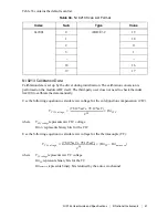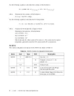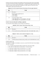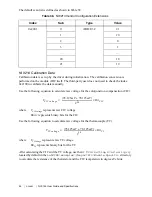
50
|
ni.com
|
NI 9144 User Guide and Specifications
Table 48.
NI 921
8
Scan List Format
Bits
Field
Description
31..22
Reserved
—
21
Offset Cal Enable <ch1>
Controls the offset calibration mode. Offset
calibration mode disconnects both signal input
pins and forces the channel inputs to zero volts,
enabling measurement of the channel offset
voltage. A logic 1 in any bit enables offset
calibration for the channel, while a logic 0
disables the offset calibration.
20
Shunt Cal Enable <ch1>
Controls the shunt calibration switch for each of
the two channels. A logic 1 in any bit closes the
switch for the respective channel, while a logic 0
opens the switch.
19..16
Module Mode Setting
<ch1>
Saves the module mode calibration information
for the channel.
15..14
Reserved
—
13
Offset Cal Enable <ch0>
Controls the offset calibration mode. Offset
calibration mode disconnects both signal input
pins and forces the channel inputs to zero volts,
enabling measurement of the channel offset
voltage. A logic 1 in any bit enables offset
calibration for the channel, while a logic 0
disables the offset calibration.
12
Shunt Cal Enable <ch0>
Controls the shunt calibration switch for each of
the two channels. A logic 1 in any bit closes the
switch for the respective channel, while a logic 0
opens the switch.
11..8
Module Mode Setting
<ch1>
Saves the module mode calibration information
for the channel.
7
Reserved
6..2
Clock Divisor
The NI 9218 divides the clock source by this
value and uses it as the converters’ oversample
clock. The data rate is equal to 1/256 times this
oversample clock frequency.
1..0
Clock Source
—


