background image

16

|

ni.com

|

NI PXIe-4463 Calibration Procedure

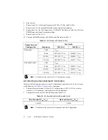
b.

Call 

Basic Function Generator

 using the parameters in Table 20.

c.

Write the resulting waveform to AO, and start the task.

4.

Measure the output current with the DMM.

5.

Stop the task.

6.

Repeat steps 1 to 5 for AO 1.

7.

Compare the results with the following test limit (min):

output current

70.71 mA

rms

Timebase Frequency Accuracy Verification

Note

Both analog outputs on a single device use the same timebase circuitry. 

Therefore, the measurements made on one channel are valid for both channels.

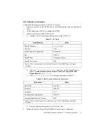
Complete the following procedure to verify the timebase frequency accuracy.
1.

Connect channel AO 0 of the NI PXIe-4463 to the frequency counter using the cables 
recommended in Table 1.

2.

Configure the frequency counter using the values in Table 21.

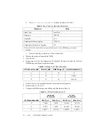
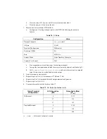
Table 20.  

Basic Function Generator Parameters

Parameter

Value

Signal Type

Sine Wave

Frequency

100 Hz

Amplitude

4.5 V

Sampling Info»Sampling Rate

51200 S/s

Sampling Info»Number of Samples

512

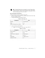
Table 21.  

Frequency Counter Setup

Configuration

Value

Function

Frequency

Impedance

1 M

Range

50 V

Coupling

AC

Bandwidth Limit

100 kHz

Trigger Source

Internal

Gate Time

0.5 s

Summary of Contents for NI PXIe-4463

Page 1: ... Test Equipment 3 Test Conditions 5 Initial Setup 6 Self Calibration 6 Verification 6 Analog Output Performance Verification 7 AO Offset Accuracy Verification 7 AO Gain Accuracy Verification 9 AO Flatness Verification 11 AO Interchannel Gain Mismatch Verification 12 AO Noise Verification 13 AO Current Drive Verification 15 Timebase Frequency Accuracy Verification 16 Adjustment 18 AO Offset and Gai...

Page 2: ...ations all functions used in verification and adjustment procedures can be found in the LabVIEW Functions palette C C equivalents are referenced in parentheses Documentation Consult the following documents for information about the NI PXIe 4463 NI DAQmx and your application software All documents are available on ni com and help files install with the software NI PXIe 4463 Getting Started Guide NI...

Page 3: ... information for NI DAQmx NET methods and NI DAQmx NET properties key concepts and a C enum to NET enum mapping table Table 1 Required Equipment Equipment Recommended Model Where Used Requirements Digital Multimeter DMM Keysight Technologies 3458A AO Offset Verification AO Offset and Gain Adjustment DC Voltage Input Range 1 V 10 V Accuracy 2 ppm of range 15 ppm of reading AO Gain Verification AO F...

Page 4: ...Verification Noise 0 7 µVrms PXI Express Chassis NI PXIe 1082 All Tests One of the following chassis NI PXIe 1082 NI PXIe 1085 NI PXIe 1075 NI PXIe 1065 NI PXIe 1062Q System Controller NI PXIe 8135 All Tests A PXI Express controller or MXI Express card mXLR F to BNC M Cable quantity 1 NI 156789 0R46 or NI 140150 0R46 All Tests mXLR Variant Length 0 5 m BNC M to BNC M Cable quantity 1 Pomona Electr...

Page 5: ...I PXIe 4463 temperature will be greater than the ambient temperature As Found Test Limits are valid for a device temperature within 5 C of the last self calibration Keep relative humidity below 80 Allow a warm up time of at least 15 minutes to ensure that the NI PXIe 4463 circuitry is at a stable operating temperature Allow adequate warm up time for all of the instruments and equipment according t...

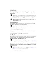
Page 6: ... minutes for the device to warm up 2 Launch MAX 3 Select My System Devices and Interfaces and then select the NI PXIe 4463 device to self calibrate 4 Click Self Calibrate in the upper right corner of the window Verification The following procedures describe the sequence of operation and provide test points required to verify the NI PXIe 4463 The verification procedures assume that adequate traceab...

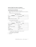
Page 7: ...tion in Table 2 3 Generate a voltage with the NI PXIe 4463 a Configure an AO voltage channel task using the values in Table 3 b Create an array of 512 points and fill every element with value 0 c Write the array to AO and start the task 4 Measure the output voltage with the DMM 5 Stop the task Table 2 DMM Configuration Configuration Value Function DC Volts DCV Range 1 V Number of Power Line Cycles...

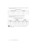
Page 8: ...epeat steps 1 to 7 for AO 1 9 Compare each measured value with the Min and Max limits in Table 5 Note Test limits are the same for differential and pseudodifferential output configurations Table 4 AO Attenuation AO Attenuation dB AO Gain dB 0 0 17 17 37 37 Table 5 AO Offset Verification Limits AO Attenuation dB As Found Test Limits As Left Test Limits Min mV Max mV Min mV Max mV 0 0 5 0 5 0 22 0 2...

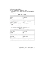
Page 9: ...the values in Table 7 Table 6 DMM Configuration Configuration Value Function AC Volts ACV Range 10 V RMS Mode SETACV 3 SYNC AC Bandwidth ACBAND 20 100000 20 Hz to 100 kHz Level Filter LFILTER 1 ON Refer to Table 9 for details about the correlation between AO Gain DMM Range and Signal Amplitude Table 7 AO Setup Configuration Value Physical Channels Dev_name ao0 AO Gain 0 dB Output Terminal Configur...

Page 10: ...ax and Min limits in Table 10 Table 8 Basic Function Generator Parameters Parameter Value Signal Type Sine Wave Frequency 1000 Hz Amplitude 10 V Sampling Info Sampling Rate 51200 S s Sampling Info Number of Samples 512 Refer to Table 9 for details about the correlation between AO Gain DMM Range and Signal Amplitude Table 9 Settings for AO Gain Verification AO Attenuation dB AO Gain dB DMM Range V ...

Page 11: ...all Basic Function Generator using the parameters in Table 12 d Write the resulting waveform to AO and start the task 4 Measure the output voltage with the DMM and record for future calculations Table 11 AO Setup Configuration Value Physical Channels Dev_name ao0 AO Gain 0 dB Output Terminal Configuration Differential Rate 51200 S s Sample Mode Continuous Sample Samples Per Channel 2560 Refer to T...

Page 12: ...recorded during AO Flatness Verification for calculations 1 Compute the ratio between AO 0 and AO 1 output voltages AO 0 AO 1 for each test frequency AO Attenuation and Output Terminal Configuration 2 Compare the results with the Min and Max limits in Table 14 Note Test limits are the same for all frequencies and AO configurations Table 13 AO Flatness Verification Limits Output Terminal Configurat...

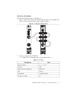
Page 13: ...n Figure 1 Figure 1 AO Noise Verification Setup 2 Generate a voltage with the NI PXIe 4463 a Configure an AO voltage channel task using the values in Table 15 Table 15 AO Setup Configuration Value Physical Channels Dev_name ao0 AO Gain 0 dB Output Terminal Configuration Differential Rate 51200 S s Sample Mode Continuous Sample Samples Per Channel 512 NI PXIe 4464 DSA Analog Input AI 0 AI 1 AI 2 AI...

Page 14: ...array Obtain the noise as standard deviation output 4 Stop all previously started tasks 5 Repeat steps 2 to 4 for AO Attenuation of 17 dB and 37 dB 6 Repeat steps 2 to 5 for pseudodifferential output terminal configuration 7 Repeat steps 1 to 6 for AO 1 8 Compare the results with the limits in Table 17 Table 16 AI Setup Configuration Value Physical Channels Dev_name ai0 3 AI Gain 30 dB Terminal Co...

Page 15: ... the AO current drive 1 Connect channel AO 0 of the NI PXIe 4463 to the DMM current measurement ports using the cables recommended in Table 1 2 Configure the DMM using the information in Table 18 3 Generate a waveform with NI PXIe 4463 a Configure an AO voltage channel task using the values in Table 19 Table 18 DMM Configuration Configuration Value Function AC Current ACI Range 0 1 A Number of Pow...

Page 16: ...measurements made on one channel are valid for both channels Complete the following procedure to verify the timebase frequency accuracy 1 Connect channel AO 0 of the NI PXIe 4463 to the frequency counter using the cables recommended in Table 1 2 Configure the frequency counter using the values in Table 21 Table 20 Basic Function Generator Parameters Parameter Value Signal Type Sine Wave Frequency ...

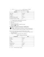
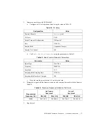
Page 17: ...5 Stop the task Table 22 AO Setup Configuration Value Physical Channels Dev_name ao0 AO Gain 0 dB Output Terminal Configuration Differential Rate 51200 S s Sample Mode Continuous Sample Samples Per Channel 500 Table 23 Basic Function Generator Parameters Parameter Value Signal Type Sine Wave Frequency 20480 Hz Amplitude 10 V Sampling Info Sampling Rate 51200 S s Sampling Info Number of Samples 500...

Page 18: ...refer to the instructions in the EEPROM Update section The following procedures describe the sequence of operation required to adjust the NI PXIe 4463 AO Offset and Gain Adjustment Complete the following procedure to adjust the offset and gain performance of the NI PXIe 4463 Note Set the polymorphic selector to 4463 for all polymorphic VIs used in the Offset and Gain Adjustment procedure 1 Connect...

Page 19: ... the session Use the action cancel if there has been any error during the calibration or if you do not want to save the new calibration constants in the device EEPROM Use the action commit if you want to save the new calibration constants in the device EEPROM Timebase Adjustment Complete the following procedure to adjust the timebase frequency of the NI PXIe 4463 Note Set the polymorphic selector ...

Page 20: ...or verification before adjustment and As Left limits for verification after adjustment Note If any test fails reverification confirm that you have met the Test Conditions before returning your device to NI Refer to Worldwide Support and Services for assistance in returning the device to NI Worldwide Support and Services The National Instruments website is your complete resource for technical suppo...

Page 21: ... policy and how to obtain relevant HTS codes ECCNs and other import export data NI MAKES NO EXPRESS OR IMPLIED WARRANTIES AS TO THE ACCURACY OF THE INFORMATION CONTAINED HEREIN AND SHALL NOT BE LIABLE FOR ANY ERRORS U S Government Customers The data contained in this manual was developed at private expense and is subject to the applicable limited rights and restricted data rights as set forth in F...

Reviews: