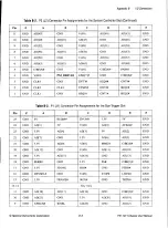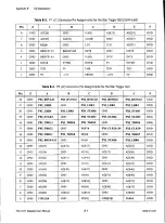
I/O Connectors
Pin
Z
A
B
C
D
E
F
25
GND
5V
REQ64#
ENUM#
3.3V
5V
GND
24
GND
AD[1]
5V
V(1/0)
AD[0]
ACK64#
GND
23
GND
3.3V
AD[4]
AD[3]
5V
AD[2]
GND
22
GND
AD[7]
GND
3.3V
AD[6]
AD[5]
GND
21
GND
3.3V
AD[9]
AD[8]
M66EN
C/BE[0]#
GND
20
GND
AD[12]
GND
V(1/0)
A D [ l l ]
AD[10]
GND
19
GND
3.3V
AD[15]
AD[141
GND
AD[13]
GNI)
18
GND
SERR#
GND
3.3V
PAR
C/BE[1]#
GND
This appendix describes the
PXI subsystem backplane.
Table B-1 shows the PI (J1)
Controller slot.
Table B-2 shows the P2 (J2)
Controller slot.
Table B-3 shows the PI (J1)
Trigger slot.
Table B-4 shows the P2 (J2)
Trigger slot.
Table B-5 shows the P1
(J1)
peripheral slots.
Table B-6 shows the P2 (J2)
peripheral slots.
Note
P X I signals are shown in
bold.
PI
and P2 connector pin assignments for the
connector pin assignments for the System
connector pin assignments for the System
connector pin assignments for the Star
connector pin assignments for the Star
connector pin assignments for the
connector pin assignments for the
Table B-1.
P1 (J1) Connector Pin Assignments for the System Controller Slot
© National Instruments Corporation
B-1
PXI-1011 Chassis User Manual

