Chapter 1
Getting Started
1-12
ni.com
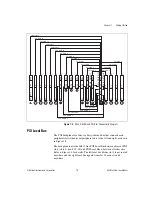
Figure 1-5.
Distribution of PXI_CLK10, PXIe_CLK100, and PXIe_SYNC100
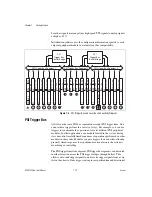
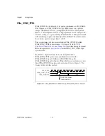
PXI_CLK10, PXIe_CLK100 and PXIe_SYNC100 have the default timing
relationship described in Figure 1-6.
Figure 1-6.
System Reference Clock Default Behavior
To synchronize the system to an external clock, you can drive PXI_CLK10
from an external source through the PXI_CLK10_IN pin on the System
Timing Slot. Refer to Table B-8,
XP4 Connector Pinout for the System
, for the pinout. When a 10MHz clock is detected on this pin,
the backplane automatically phase-locks the PXI_CLK10, PXIe_CLK100,
and PXIe_SYNC100 signals to this external clock and distributes these
P2
P1
XP4
XP
3
TP2
TP1
P2
P1
P2
P1
P2
P1
P1
P1
P1
XP4
XP
3
XP4
XP
3
XP4
XP
3
XP4
XP
3
XP4
XP
3
XP4
XP
3
XP4
XP
3
P2
P1
P2
P1
P2
P1
P2
P1
P2
P1
XP4
XP
3
XP2
XP1
P1
10 MHz
REF IN
10 MHz
REF OUT
PXI_CLK10_IN
1
8
9
10
PXIe_CLK100
PXIe_
S
YNC100
PXI_CLK10
7
H
11
H
H
12
H
1
3
14
15
6
5
4
3
2
16
17
1
8
PXIe_CLK100
PXI_CLK10
PXIe_
S
YNC100
0 1 2
3
4 5 6 7
8
9 0 1 2
3
4 5 6 7
8
9 0 1 2
3
4 5 6 7
8
9


