Chapter 1
Getting Started
1-8
ni.com
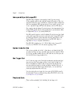
System Reference Clock
The PXI-1052 supplies the PXI 10 MHz system clock signal (PXI_CLK10)
independently to each peripheral slot. An independent buffer (having a
source impedance matched to the backplane and a skew of less than 500 ps
between slots) drives the clock signal to each peripheral slot. You can use
this common reference clock signal to synchronize multiple modules in a
measurement or control system. You can drive PXI_CLK10 from an
external source through the PXI_CLK10_IN pin on the P2 connector of the
star trigger slot. Refer to Table B-4,
P2 (J2) Connector Pinout for the Star
. Sourcing an external clock on this pin automatically overrides
the 10 MHz source of the backplane. Once the transition has been made,
reset the chassis to restore it to the initial state.
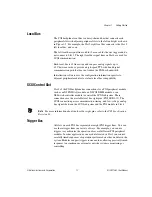
Figure 1-3.
PXI Star Trigger and Local Bus Routing
SCXI Subsystem Overview
To use the SCXI subsystem of the PXI-1052, you
must
have a
DAQ/DMM/Switch controller module in Slot 4 of the PXI subsystem
to control and/or acquire data from the SCXI modules.
Note
The chassis address of the SCXI subsystem is hard-wired as 0.
PXI Trigger Bus Segment and PCI Bus Segment
1
SCXI
Connection
System Controller
Star T
rigger
Controller
2
3
4
System Reference Clock Buffer and Detection Circuitry
PXI Star Triggers
Local
Bus
Local
Bus


